GaN Gunn diode based on AlGaN electro emission layer with bilinear-gradient Al components and manufacturing method of GaN Gunn diode

An electron emission layer, Gunn diode technology, applied in circuits, electrical components, bulk negative resistance effect devices, etc. The effect of reducing the dislocation concentration

Active Publication Date: 2014-08-27
云南凝慧电子科技有限公司
View PDF2 Cites 4 Cited by
  • Summary
  • Abstract
  • Description
  • Claims
  • Application Information

AI Technical Summary

Problems solved by technology

However, the AlGaN electron emission layer structures involved in current literature reports have failed to balance the two factors of dislocation filtering and lat

Method used


Image

  • GaN Gunn diode based on AlGaN electro emission layer with bilinear-gradient Al components and manufacturing method of GaN Gunn diode
  • GaN Gunn diode based on AlGaN electro emission layer with bilinear-gradient Al components and manufacturing method of GaN Gunn diode
  • GaN Gunn diode based on AlGaN electro emission layer with bilinear-gradient Al components and manufacturing method of GaN Gunn diode

Examples


Embodiment 1

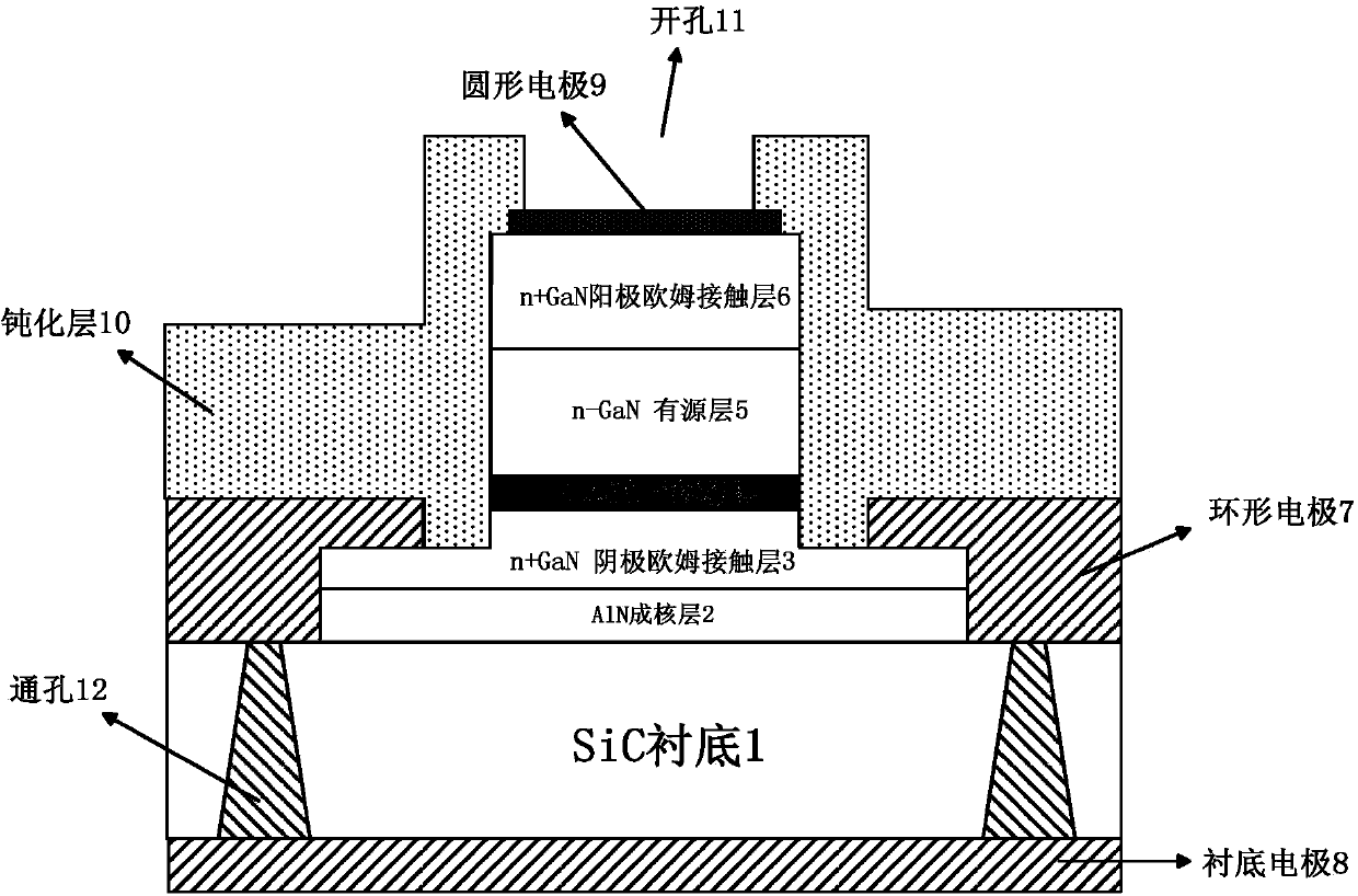
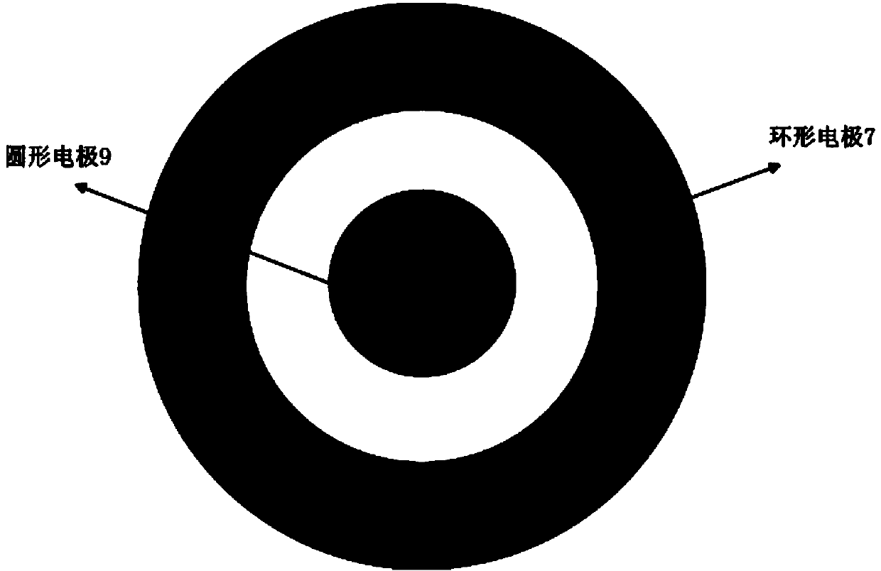
[0042] Embodiment 1: Fabricate a GaN Gunn diode on a 4H-SiC semi-insulating substrate.

[0043] Step 1, select a 4H-SiC semi-insulating substrate with a diameter of 2 inches, and thin the back surface until the thickness of the substrate is 150um.

[0044] Step 2, put the 4H-SiC semi-insulating substrate into the MOCVD reaction chamber, set the growth temperature to 600°C, feed trimethylaluminum and nitrogen into the reaction chamber at the same time, and grow under the condition of maintaining the pressure at 40 Torr AlN nucleation layer with a thickness of 30 nm.

[0045] Step 3: Raise the substrate on which the AlN nucleation layer has been grown to 1000°C, simultaneously inject trimethylgallium, nitrogen and n-type dopant source-silane into the reaction chamber, and keep the pressure at 40Torr , with a growth thickness of 100 nm and a doping concentration of 1.0×10 18 cm -3 the n + GaN cathode ohmic contact layer.

[0046] Step 4, the air pressure in the MOCVD reactio...

Embodiment 2

[0057] Embodiment 2: Fabricate a GaN Gunn diode on a 6H-SiC semi-insulating substrate.

[0058] Step 1, thinning the substrate

[0059] A 6H-SiC semi-insulating substrate with a diameter of 2 inches is selected, and the back surface is thinned until the thickness of the substrate is 150um.

[0060] Step 2, epitaxial growth of AlN nucleation layer

[0061] Using MOCVD, under the conditions of maintaining a pressure of 40Torr and a temperature of 650°C, trimethylaluminum and nitrogen are fed simultaneously to grow an AlN nucleation layer with a thickness of 40nm on a 6H-SiC semi-insulating substrate.

[0062] Step three, epitaxial growth n + GaN cathode ohmic contact layer

[0063] Using MOCVD, raise the temperature to 1060°C, keep the pressure at 40Torr, and feed trimethylgallium, nitrogen and n-type dopant source—silane at the same time, the epitaxial growth thickness is 150nm, and the doping concentration is 1.5 ×10 18 cm -3 the n + GaN cathode ohmic contact layer.

...

Embodiment 3

[0091] Embodiment 3: Fabricate a GaN Gunn diode on a 6H-SiC conductive substrate.

[0092] Step A, thinning the substrate

[0093] A 6H-SiC conductive substrate with a diameter of 2 inches is selected, and the back surface is thinned until the thickness of the substrate is 150um.

[0094] Step B, making AlN nucleation layer and n + GaN cathode ohmic contact layer

[0095] In the MOCVD reaction chamber, under the conditions of keeping the pressure at 60 Torr and the temperature at 650°C, feed trimethylaluminum and nitrogen at the same time, and grow an AlN nucleation layer with a thickness of 90nm on the 6H-SiC conductive substrate; continue Using MOCVD process, raise the temperature to 1100℃, keep the pressure at 60Torr, and then feed trimethylgallium, nitrogen and n-type dopant source - silane at the same time, and epitaxially grow n + GaN cathode ohmic contact layer, the thickness of the ohmic contact layer is 400nm, and the doping concentration is 2×10 18 cm -3 .

[0...


PUM

PropertyMeasurementUnit
Thicknessaaaaaaaaaa
Thicknessaaaaaaaaaa
Thicknessaaaaaaaaaa

Abstract

The invention discloses a GaN Gunn diode based on an AlGaN electro emission layer with bilinear-gradient Al components and a manufacturing method of the GaN Gunn diode. The GaN Gunn diode and the manufacturing method of the GaN Gunn diode mainly solve the problems that an existing Gunn device is low in output power and poor in heat dissipation performance. The diode comprises a main part and an auxiliary part. The main part comprises an SiC substrate, an AlN coring layer, an n+GaN cathode ohmic contact layer, an electro emission layer, an n-GaN active layer and an n+GaN anode ohmic contact layer from bottom to top and the auxiliary part comprises an annular electrode, a substrate electrode, a round electrode, a passivation layer, open holes and through holes, wherein the thickness of the electro emission layer is 200-600 nm, and the AlGaN structure with the bilinear-gradient Al components which are gradually changed linearly from 0% to 100% firstly and then from 100% to 0% from bottom to top is adopted. By means of the GaN Gunn diode and the manufacturing method of the GaN Gunn diode, the length of a dead zone can be obviously reduced, the dislocation concentration can be reduced and high-power output can be realized, and the GaN Gunn diode is suitable for working in the terahertz frequency range.

Description

technical field [0001] The invention belongs to the technical field of microelectronic devices, and in particular relates to a Gunn diode made of GaN semiconductor material with a wide bandgap, which can be used for making high-frequency and high-power devices. technical background [0002] As a new type of wide-bandgap semiconductor, GaN material has the characteristics of large bandgap width, stable chemical properties, high critical breakdown electric field, high electron saturation velocity, and high concentration of heterojunction two-dimensional electron gas. It is widely used in millimeter wave high-power electronic devices. field has received extensive attention. Compared with the traditional III-V compound semiconductor GaAs, the negative resistance oscillation fundamental frequency of GaN reaches 750GHz, far exceeding GaAs's 140GHz. In addition, the output power of GaN-based electronic devices is also higher than that of GaAs-based electronic devices. 1 to 2 order...

Claims


Application Information

Patent Timeline
IPC IPC(8): H01L47/02H01L47/00
Inventor 杨林安许详李亮张进成郝跃
Owner 云南凝慧电子科技有限公司
Why Eureka
Try Eureka