A microfluidic chip for nucleic acid sequencing

A microfluidic chip and nucleic acid sequencing technology, applied in laboratory containers, enzymology/microbiology devices, specific-purpose bioreactors/fermenters, etc., can solve problems such as expensive raw materials and complex substrate modification, Achieve the effects of saving reagent consumption, high reaction and washing efficiency, and improving accuracy

Active Publication Date: 2016-04-06
南京环朋医疗技术有限公司
View PDF6 Cites 0 Cited by
  • Summary
  • Abstract
  • Description
  • Claims
  • Application Information

AI Technical Summary

Problems solved by technology

[0008] Despite the rapid development of sequencing technology, all current sequencing platforms are chip-based biomolecular detection. Chip design and preparation are crucial to the efficiency and speed of sequencing. Currently, mainstream chips are mainly microfluidic channels and micropore structures. , and requires complex substrate modification and expensive raw materials

Method used


Image

  • A microfluidic chip for nucleic acid sequencing
  • A microfluidic chip for nucleic acid sequencing
  • A microfluidic chip for nucleic acid sequencing

Examples


Embodiment 1

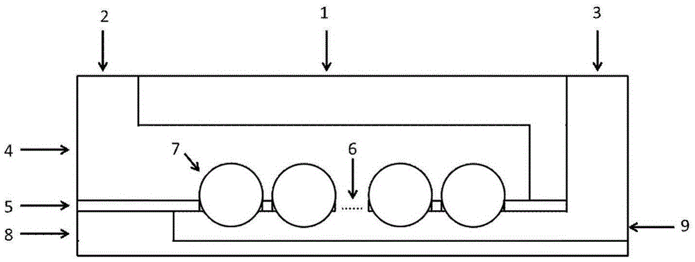
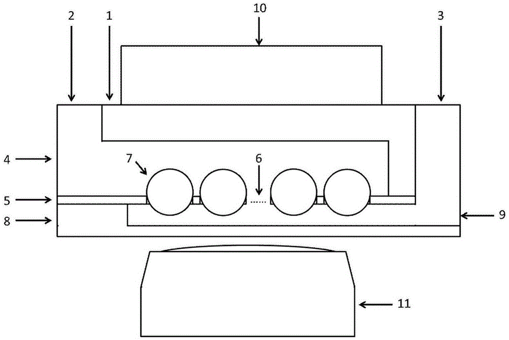
[0041] a) Preparation of the upper layer chip: use a 3cm×7cm quartz plate, cut out three microchannels with a length of 5.2cm, a width of 5mm, and a depth of 50μm in the quartz plate through laser micromachining, and the interval between the three channels is 2mm, and a diameter of 1mm is punched out. Liquid outlet and inlet.

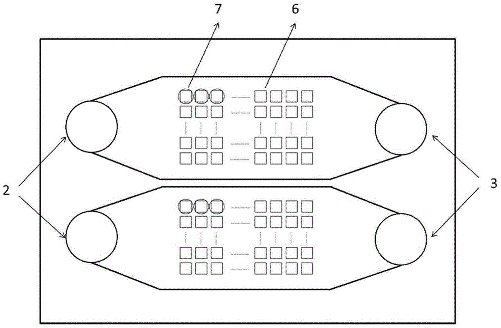
[0042] b) Fabrication of the middle layer chip: use a 3cm×7cm metal nickel film to obtain a square through-hole microarray by electrochemical etching at the position corresponding to the microchannel of the upper chip. The edge of the microwell array is 4 μm from the edge of the channel, and 2 mm from the entrance and exit of the channel.

[0043] c) Preparation of the lower layer chip: using a 3 cm x 7 cm quartz plate, three microchannels with a length of 5.2 cm, a width of 5 mm and a depth of 50 μm were cut out in the quartz plate by laser micromachining.

[0044] d) Chip assembly: The three-layer chip is connected together by 5 μm thick glue, and co...

Embodiment 2

[0047] a) Preparation of the upper chip: use a 3cm×7cm silicon wafer, and prepare three microchannels with a length of 5.2cm, a width of 5mm, and a depth of 20μm in the silicon wafer by wet etching. The three channels are separated by 2mm and the diameter is 1mm. liquid outlet and inlet.

[0048] b) Preparation of the middle layer chip: use a 3cm×7cm silicon wafer, and dry-etch a square through-hole microarray at the position corresponding to the microchannel of the upper chip. The edge of the hole array is 4 μm away from the edge of the channel, and 2 mm away from the entrance and exit of the channel.

[0049] c) Preparation of the lower layer chip: using a 3 cm x 7 cm quartz plate, three microchannels with a length of 5.2 cm, a width of 5 mm and a depth of 20 μm were cut out in the quartz plate by laser micromachining.

[0050] d) Chip assembly: The three-layer chip is connected together through a bonding process, and connected to the peripheral pipeline through the liquid ...

Embodiment 3

[0053] a) Preparation of the upper layer chip: use a 3cm×7cm silicon wafer, and print adhesive glue containing 3 microchannels with a length of 5.2cm, a width of 5mm, and a depth of 100μm on the quartz wafer through a screen printing process. The three channels are spaced at 2mm, and Make a liquid outlet and inlet with a diameter of 1mm.

[0054] b) Preparation of the middle layer chip: use a 3cm×7cm silicon wafer, and wet-etch at the position corresponding to the microchannel of the upper chip to obtain a square through-hole microarray. The edge of the microwell array is 4 μm from the edge of the channel, and 2 mm from the entrance and exit of the channel.

[0055] c) Preparation of the lower layer chip: use a 3cm×7cm glass sheet, and print adhesive glue containing 3 microchannels with a length of 5.2cm, a width of 5mm, and a depth of 100μm on the quartz sheet by a screen printing process, and the distance between the three channels is 2mm.

[0056] d) Chip assembly: the thr...


PUM


Abstract

The invention aims to provide a micro-fluidic chip for nucleic acid sequencing. The chip comprises a group of reaction tanks formed by multiple micro-fluidic channels. The micro-fluidic chip mainly consists of three layers of structures, wherein an upper chip 1 is a solid material substrate, and a liquid inlet 2, a liquid outlet 3 and an upper micro-channel groove 4 are formed in the surface of the upper chip; a square through hole micro array 6 is formed in a middle chip 5, and a microsphere 7 fixedly provided with a sequencing template is captured in each square through hole; a bottom chip 8 is a transparent solid material substrate, and a lower micro-channel groove 9 is formed in the surface of the bottom chip. In the chip application process, the sequencing template is fixed on each microsphere, and a sequencing reaction solution and a washing solution flow through the micro through hole array from pores between the microspheres and the square through holes. The chip is simple in design and structure and easy to prepare, the microspheres are fixed, the reacting and washing speed is accelerated, the amount of reagents is reduced, and the washing effect is enhanced, so that the nucleic acid sequencing cost is reduced, and the sequencing time is shortened.

Description

technical field [0001] The invention relates to a microfluidic chip for nucleic acid sequencing. It can be widely used in the fields of nucleic acid sequencing, gene mutation detection and molecular diagnosis. Background technique [0002] Since the emergence of Sanger nucleic acid sequencing technology in the mid-1970s, nucleic acid sequencing technology has made great progress, especially with the completion of the Human Genome Project, nucleic acid sequencing technology has greatly changed the research landscape in many fields of life sciences. [0003] As the first-generation sequencing technology, Sanger sequencing is convenient, simple, highly reliable, and has long sequencing fragments. It has also become the sequencing technology used in human genome sequencing. However, Sanger sequencing cannot be further miniaturized, and the sequencing throughput is also limited. With the development and in-depth research of related biotechnology, DNA sequencing technology has al...

Claims


Application Information

Patent Timeline
Patent Type & Authority Patents(China)
IPC IPC(8): C12M1/34
CPCB01L3/502761B01L2300/0819B01L2300/0887
Inventor 赵祥伟葛芹玉顾忠泽
Owner 南京环朋医疗技术有限公司
Why Eureka
Try Eureka