Polysilicon resistor structure and method of forming the same

A polysilicon resistor and resistor technology, applied in circuits, electrical components, electrical solid devices, etc., can solve the problems of unstable electrical characteristics and high temperature of integrated circuits, and improve the temperature stability of resistance, reduce the variation range, and improve temperature stability. Effect

Active Publication Date: 2017-05-24
SEMICON MFG INT (SHANGHAI) CORP
View PDF1 Cites 0 Cited by
  • Summary
  • Abstract
  • Description
  • Claims
  • Application Information

AI Technical Summary

Problems solved by technology

[0010] However, with the increase in the integration of semiconductor devices, the temperature in semiconductor integrated circuits is also getting higher and higher, and the polysilicon resistance will have a high temperature due to the self-heating effect when it is working.
Since the polysilicon material changes with temperature, when the polysilicon resistor is working, the resistance value of the corresponding polysilicon resistor will change accordingly, making the electrical characteristics of the integrated circuit unstable

Method used


Image

  • Polysilicon resistor structure and method of forming the same
  • Polysilicon resistor structure and method of forming the same
  • Polysilicon resistor structure and method of forming the same

Examples


no. 1 example

[0041] Please refer to Figure 7 ~ Figure 11 , is a schematic cross-sectional structure diagram of the formation process of the polysilicon resistance structure according to the first embodiment of the present invention.

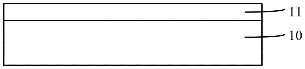
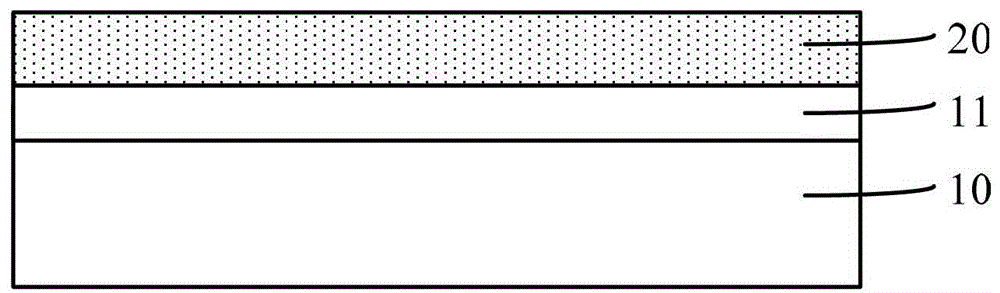
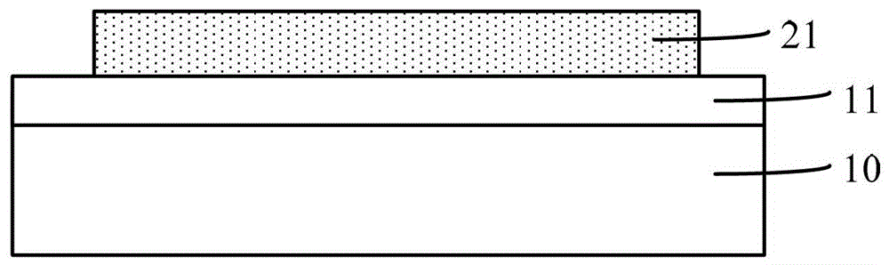
[0042] Specifically, please refer to Figure 7 , a substrate 100 is provided, and an isolation layer 101 is formed on the surface of the substrate 100 .

[0043] The substrate 100 can be a semiconductor substrate such as a bulk silicon substrate, a bulk germanium substrate, a silicon germanium substrate, a silicon carbide substrate, a silicon-on-insulator substrate, or a germanium-on-insulator substrate, or a ruby ​​substrate, a sapphire substrate, etc. Insulating substrates such as substrates and glass substrates.

[0044] In this embodiment, the substrate 100 is a bulk silicon substrate. Since the bulk silicon substrate is doped with impurity ions, it has conductivity. Therefore, before forming the polysilicon resistor, the bulk silicon substrate and the...

no. 2 example

[0092] In the second embodiment of the present invention, a polysilicon resistor, a first metal silicide layer, a second metal silicide layer, a first interlayer dielectric layer, a first conductive plug, a second conductive plug, a first metal layer, and a second conductive plug are formed. The formation process of the second metal layer is consistent with the formation process in the first embodiment, please refer to the first embodiment Figure 7 ~ Figure 11 , which will not be described here.

[0093] Please also refer to Figure 11 with Figure 12 After forming the first metal layer 122 and the second metal layer 132, a second interlayer dielectric layer 160 is formed on the surfaces of the first metal layer 122, the second metal layer 132 and the first interlayer dielectric layer 150, and A third conductive plug 123 is formed in the second interlayer dielectric layer 160 and on the surface of the first metal layer 122, and a top metal layer is formed on the surface of ...


PUM


Abstract

The invention relates to a polyresistor structure and a forming method thereof. The polyresistor structure comprises a substrate, a polyresistor, a metal electrode, and a metal heat radiation structure; the polyresistor with the resistor negative temperature coefficient is arranged at the substrate; the metal electrode is electrically connected with the two ends of the polyresistor; and the metal heat radiation structure with the resistor positive temperature coefficient is arranged at the surface of the middle portion of the polyresistor. The metal heat radiation structure is isolated from the metal electrode, so that the total resistance changing amplitude of the polyresistor structure is reduced when the temperature changes. Because the heat generated by the polyresistor can be dissipated by the metal heat radiation structure, the temperature changing amplitude of the polyresistor structure during working can be reduced beneficially, thereby reducing the changing value of the total resistance value of the polyresistor structure with the temperature can be reduced. Moreover, on the basis of the metal interconnection structure with the resistor positive temperature coefficient, the changing value of the total resistance value of the polyresistor structure with the temperature can also be reduced, thereby improving the temperature stability of the resistance value of the polyresistor structure beneficially.

Description

technical field [0001] The invention relates to the field of semiconductor manufacturing, in particular to a polysilicon resistance structure and a forming method thereof. Background technique [0002] In semiconductor integrated circuits (ICs), polysilicon resistors are a very commonly used electronic component. According to different doping ions and doping levels, P+, N+, P- and N- polysilicon resistors can be manufactured. For the formation process of existing polysilicon resistors, please refer to Figure 1 to Figure 6 ,include: [0003] Please refer to figure 1 , providing a semiconductor substrate 10, and forming an insulating layer 11 on the semiconductor substrate 10; [0004] Please refer to figure 2 , forming a polysilicon film 20 on the surface of the insulating layer 11, and performing ion doping on the polysilicon film 20; [0005] Please refer to image 3 , etching the polysilicon film 20 to form strip-shaped polysilicon resistors 21; [0006] Please r...

Claims


Application Information

Patent Timeline
Patent Type & Authority Patents(China)
IPC IPC(8): H01L27/06H01L21/02
Inventor 廖淼陈芳
Owner SEMICON MFG INT (SHANGHAI) CORP
Why Eureka
Try Eureka