LED (Light-Emitting Diode) flip chip and manufacturing method thereof

A technology of flip chip and manufacturing method, which is applied in the direction of electrical components, circuits, semiconductor devices, etc. It can solve the problems of flip chip brightness decrease, chip turn-on voltage rise, contact resistance rise, etc., and achieve low turn-on voltage and contact resistance. , good reliability effect

Inactive Publication Date: 2014-09-10
江苏汉莱科技有限公司
View PDF4 Cites 15 Cited by
  • Summary
  • Abstract
  • Description
  • Claims
  • Application Information

AI Technical Summary

Problems solved by technology

At high temperature, the metal layer, especially silver, is prone to agglomeration, which causes the reflectivity to drop from 90% before the alloy to 40-60% after the alloy, and the brightness of the flip chip drops significantly.
On the other hand, metal alloys at lower temperatures (such as 200-400 degrees Celsius) can maintain a reflectivity above 80%, but the contact resistance with p-type GaN will increase, resulting in an increase in the chip’s turn-on voltage
Therefore, high reflectivity and low contact resistance form a pair of contradictions that are difficult for metal alloys.

Method used


Image

  • LED (Light-Emitting Diode) flip chip and manufacturing method thereof
  • LED (Light-Emitting Diode) flip chip and manufacturing method thereof

Examples


Embodiment Construction

[0028] Any feature disclosed in this specification (including any appended claims, abstract and drawings), unless expressly stated otherwise, may be replaced by alternative features which are equivalent or serve a similar purpose. Unless expressly stated otherwise, each feature is only one example of a series of equivalent or similar features.

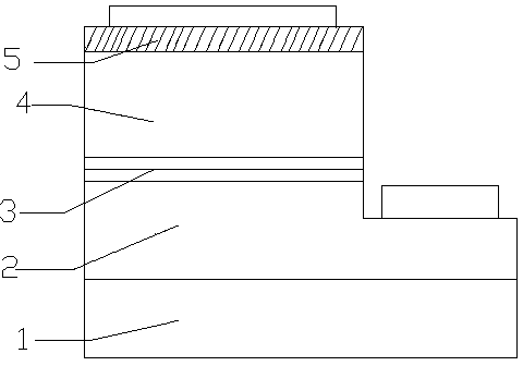
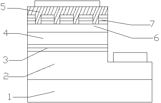
[0029] like figure 2 As shown, an LED flip chip includes a sapphire substrate 1, an LED epitaxial wafer, and an n-type GaN layer 2, a quantum well active region 3, a p-type GaN layer 4, and a metal reflector sequentially arranged on the sapphire substrate 1. layer 5, by dry etching the n-type GaN layer 2 to form an exposed region of the n-type GaN layer, and between the p-type GaN layer 4 and the metal reflection layer 5, a transparent conductive layer 6 and a dielectric reflection layer are sequentially arranged. layer 7; the material of the transparent conductive layer 6 can be indium tin oxide ITO or zinc oxide; the LED epitaxial ...


PUM


Abstract

The invention discloses an LED (Light-Emitting Diode) flip chip. The LED flip chip comprises a sapphire substrate, an LED epitaxial wafer, as well as an n type GaN layer, a quantum well active area, a p type GaN layer and a metal reflecting layer which are arranged in sequence on the sapphire substrate, wherein an n type GaN layer exposed area is formed by etching the n type GaN layer; a transparent conducting layer and a medium reflecting layer are formed in sequence between the p type GaN layer and the metal reflecting layer; the medium reflecting layer is provided with a through hole through which the metal reflecting layer extends to be connected with the transparent conducting layer; n and p electrodes are arranged on the n type GaN naked layer and the metal reflecting layer respectively. By adding the transparent conducting layer and multiple medium reflecting layers, the contradiction between the high reflectivity and low resistivity of a single metal layer is eliminated. The LED flip chip has the advantages of high light emitting rate and low startup voltage, has higher reliability, and is more suitable for use in the field of flip LEDs.

Description

technical field [0001] The invention relates to the field of manufacturing optoelectronic light-emitting devices, in particular to an LED flip chip and a manufacturing method thereof. Background technique [0002] With the rise of the third-generation semiconductor material starting from the breakthrough of P-type doping of GaN (gallium nitride) materials, the technology of high-brightness light-emitting diodes (Light Emitting Diode, LED) based on Group III nitrides Breakthroughs, nitride LEDs for a new generation of green and environmentally friendly solid-state lighting sources are becoming a new research hotspot. At present, with the continuous upgrading of LED applications and the market demand for LEDs, LEDs are developing in the direction of high power and high brightness. One of the research hotspots is LED flip-chip technology. Its structure is as figure 1 As shown, consistent with the front-mounted chip, an n-type GaN layer 2, a quantum well active region 3, and ...

Claims


Application Information

Patent Timeline
Patent Type & Authority Applications(China)
IPC IPC(8): H01L33/42H01L33/10
CPCH01L33/42H01L33/0066H01L33/0075H01L33/10H01L2933/0016
Inventor 华斌
Owner 江苏汉莱科技有限公司
Why Eureka
Try Eureka