Epitaxial gan tandem pin structure α irradiation cell and its preparation method

A tandem and epitaxy technology, applied in the field of microelectronics, can solve the problems of low energy conversion efficiency and large energy loss of incident particles, and achieve the effects of improving energy collection rate, reducing energy attenuation, and reducing energy loss

Active Publication Date: 2017-01-04
XIDIAN UNIV
View PDF1 Cites 0 Cited by
  • Summary
  • Abstract
  • Description
  • Claims
  • Application Information

AI Technical Summary

Problems solved by technology

The Schottky contact layer in the Schottky junction irradiation cell covers the entire cell area. After the incident particles reach the surface of the device, they will be blocked by the Schottky contact layer. Only part of the particles can enter the interior of the device, while those entering the depletion region The particles will contribute to the output power of the battery. Therefore, the energy loss of incident particles in this structure of the irradiation battery is large, and the energy conversion efficiency is low.

Method used


Image

  • Epitaxial gan tandem pin structure α irradiation cell and its preparation method
  • Epitaxial gan tandem pin structure α irradiation cell and its preparation method
  • Epitaxial gan tandem pin structure α irradiation cell and its preparation method

Examples


Embodiment 1

[0053] Embodiment 1, preparation α radiation source is Am 241 , a tandem PIN structure α-irradiated cell with 2 trenches of epitaxial GaN.

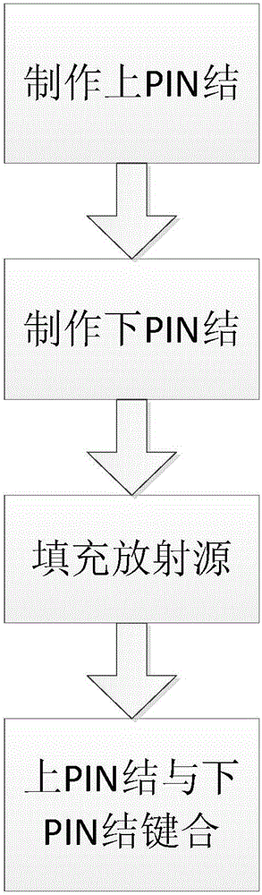
[0054] Step 1: Make the upper PIN knot.

[0055] refer to Figure 4 , the implementation of this step is as follows:

[0056] (1a) Clean the P-type SiC substrate to remove surface contaminants such as Figure 4 (a) shown.

[0057] (1a.1) Set the doping concentration to lx10 18 cm -3 P-type SiC substrate samples in NH 4 OH+H 2 o 2 Soak the sample in the reagent for 10 minutes, take it out and dry it to remove the organic residue on the surface of the sample;

[0058] (1a.2) Use HCl+H on the P-type SiC substrate after removing the surface organic residues 2 o 2 Soak the reagent for 10 minutes, take it out and dry it to remove ionic pollutants.

[0059] (1b) Epitaxial growth of P-type SiC epitaxial layer, such as Figure 4 (b) shown.

[0060] An aluminum-doped P-type doped SiC epitaxial layer is epitaxially grown on the cleaned...

Embodiment 2

[0095] Embodiment 2, preparation α radiation source is Am 241 , a tandem PIN structure α-irradiated cell with epitaxial GaN with 10 trenches.

[0096] Step 1: Make the upper PIN knot.

[0097] refer to Figure 4 , the implementation of this step is as follows:

[0098] 1) Cleaning the P-type SiC substrate to remove surface pollutants, the doping concentration of the P-type SiC substrate is lx10 18 cm -3 ,Such as Figure 4 As shown in (a):

[0099] This step is the same as step (1a) of Embodiment 1.

[0100] 2) Epitaxial growth of P-type SiC epitaxial layer, such as Figure 4 (b) shown.

[0101] An aluminum-doped P-type doped epitaxial layer is epitaxially grown on the cleaned P-type SiC substrate by chemical vapor deposition CVD. The process conditions are as follows: the epitaxy temperature is 1550°C, the pressure is 100mbar, the reaction gas is silane and propane, the carrier gas is pure hydrogen, the impurity source is trimethylaluminum, and the aluminum doping con...

Embodiment 3

[0132] Embodiment 3, preparation α radiation source is Pu 238 , a tandem PIN structure α-irradiated cell with 16 grooves.

[0133] Step A: Make the upper PIN knot.

[0134] refer to Figure 4 , the implementation of this step is as follows:

[0135] A1) cleaning the P-type SiC substrate to remove surface pollutants, the doping concentration of the P-type SiC substrate is lx10 18 cm -3 ,Such as Figure 4 As shown in (a):

[0136] This step is the same as step (1a) of Embodiment 1.

[0137] A2) Epitaxial growth of P-type SiC epitaxial layer, such as Figure 4 (b) shown.

[0138] An aluminum-doped P-type doped epitaxial layer is epitaxially grown on the cleaned P-type SiC substrate by chemical vapor deposition CVD. The process conditions are as follows: the epitaxy temperature is 1550°C, the pressure is 100mbar, the reaction gas is silane and propane, the carrier gas is pure hydrogen, the impurity source is trimethylaluminum, and the aluminum doping concentration is 3x10...


PUM


Abstract

The invention discloses an epitaxy GaN serial type PIN structure alpha irradiation battery and a manufacturing method of the epitaxy GaN serial type PIN structure alpha irradiation battery. The epitaxy GaN serial type PIN structure alpha irradiation battery mainly solves the problem that according to a silicon carbide PIN type irradiation battery manufactured in the prior art, the energy conversion efficiency is low, and the output voltage is limited and comprises an upper PIN node and a lower PIN node, and the upper PIN node and the lower PIN node are in serial connection. The upper PIN node comprises an N-type GaN epitaxial layer ohmic contact electrode, an N-type GaN epitaxial layer, a P-type SiC epitaxial layer, a P-type SiC substrate and a P-type ohmic contact electrode, and the lower PIN node comprises an N-type ohmic contact electrode, an N-type SiC substrate, an N-type SiC epitaxial layer, a P-type GaN epitaxial layer and a P-type GaN epitaxial laye ohmic contact electrode. Each PIN node comprises a plurality of grooves filled with beta irradiation sources, the epitaxial layer ohmic contact electrodes of the two PIN nodes are in contact, and the upper grooves and the lower grooves are in mirror symmetry and are communicated. The epitaxy GaN serial type PIN structure alpha irradiation battery has the advantages that the irradiation source utilization rate and energy collecting rate are high, and the output voltage of the battery is high. The battery is used for supplying power to circuits of a micro electromechanical system and the like.

Description

technical field [0001] The invention belongs to the field of microelectronics, and relates to a semiconductor device structure and a preparation method thereof, in particular to a silicon carbide-based epitaxial GaN tandem PIN structure α irradiation battery and a preparation method thereof, which can be used in micro-nano electromechanical systems and other micro Circuits and aerospace, deep sea, polar regions and other occasions that require long-term power supply and are unattended. [0002] technical background [0003] In 1953, it was discovered by Rappaport that the use of beta (β-Particle) rays produced by isotope decay can generate electron-hole pairs in semiconductors, and this phenomenon is called β-VoltaicEffect. In 1957, Elgin-Kidde first used β-VoltaicEffect in power supply and successfully manufactured the first isotope micro-battery β-VoltaicBattery. Since 1989, materials such as GaN, GaP, AlGaAs, and polysilicon have been successively used as materials for α-...

Claims


Application Information

Patent Timeline
Patent Type & Authority Patents(China)
IPC IPC(8): G21H1/06
Inventor 郭辉翟华星张艺蒙宋庆文张玉明
Owner XIDIAN UNIV
Why Eureka
Try Eureka