Manufacturing method of surface-plasmon-enhanced GaN-based nanopore LED

A surface plasmon and nanopore technology, applied in electrical components, circuits, semiconductor devices, etc., can solve the problems of difficulty in achieving luminous efficiency, low material growth quality, and large LED turn-on voltage, and achieves close coupling distance, Good electrical properties and enhanced luminous efficiency

Inactive Publication Date: 2014-09-17
INST OF SEMICONDUCTORS - CHINESE ACAD OF SCI
View PDF6 Cites 26 Cited by
  • Summary
  • Abstract
  • Description
  • Claims
  • Application Information

AI Technical Summary

Problems solved by technology

The first method is to deposit a layer of metal film or metal particles at the position of tens of nanometers on the quantum hydrazine during the growth of the epitaxial wafer to generate surface plasmon coupling. The quality of material growth in this method is not high, especially It is difficult to avoid the diffusion of metal to quantum hydrazine; the second method is to reduce the thickness of p-GaN to achieve the surface plasmon coupling distance, such as depositing a metal film or metal particles after preparing a nanopillar array. This method has cumbersome process steps. The obtained LED has a large turn-on voltage, and the loss after surface plasmon coupling is large, so it is difficult to achieve a substantial increase in luminous efficiency

Method used


Image

  • Manufacturing method of surface-plasmon-enhanced GaN-based nanopore LED
  • Manufacturing method of surface-plasmon-enhanced GaN-based nanopore LED

Examples


Embodiment Construction

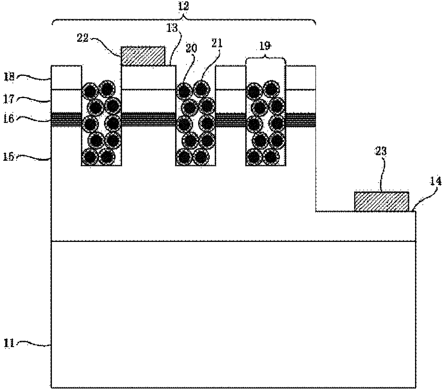
[0017] see figure 1 and figure 2 , the invention provides a method for preparing a surface plasmon-enhanced GaN-based nanohole LED, comprising the following steps:

[0018] Step 1: sequentially grow n-type In on the substrate 11 x Al y Ga z N 1-x-y-z (0≤x, y, z≤1) layer 15, undoped or doped multiple quantum well layer 16, p-type In x Al y Ga z N 1-x-y-z (0≤x, y, z≤1) layer 17 and current spreading layer 18, the material of described substrate 11 is sapphire, silicon, silicon carbide, GaN or glass, the material of described multiple quantum well layer 16 is InAlGaN / InAlGaN, the period is 2-10, and the material of the current spreading layer 18 is ITO, single-layer or multi-layer graphene;

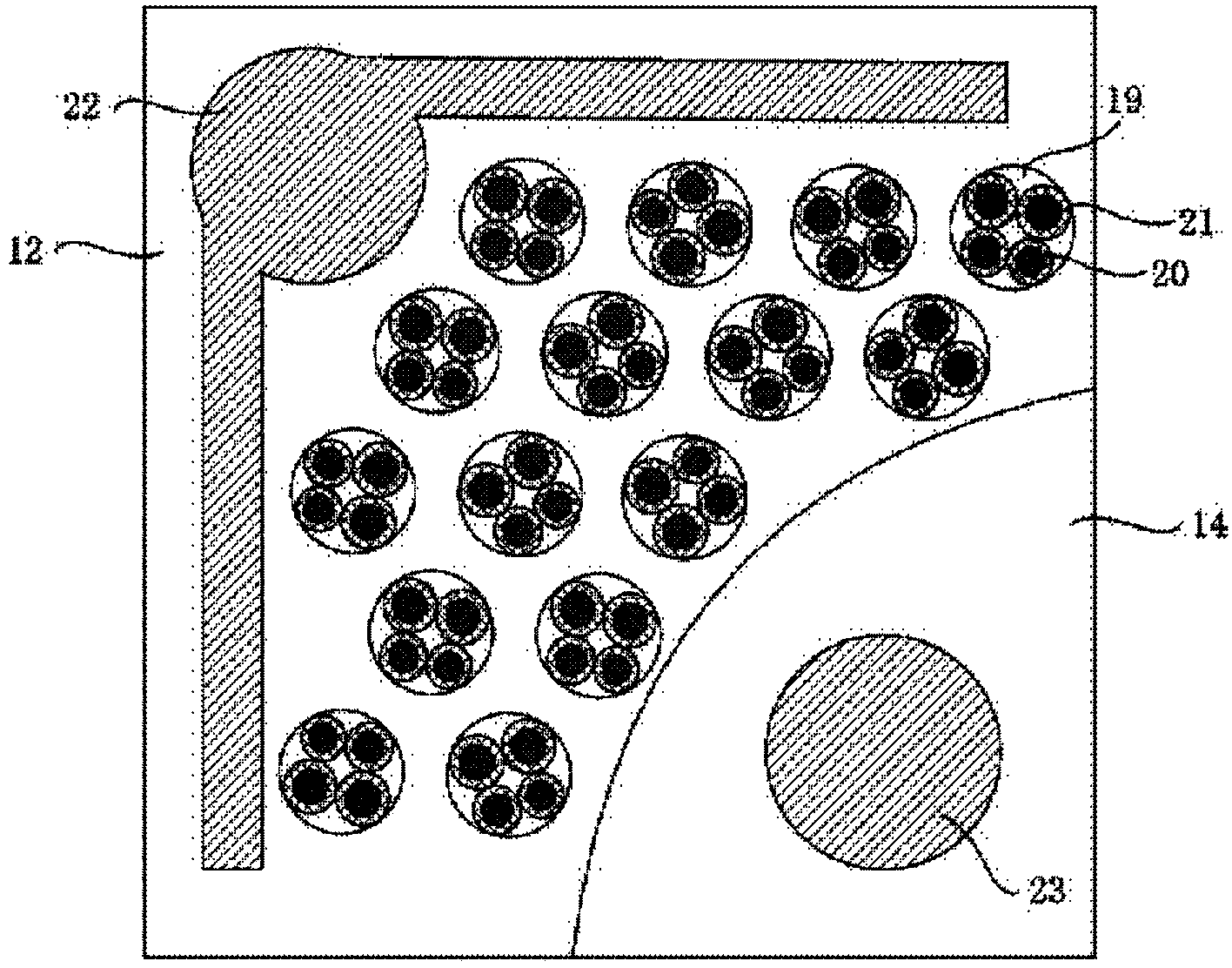
[0019] Step 2: use photolithography and dry etching process to etch downward on the current spreading layer 18, and the etching depth reaches n-type In x Al y Ga z N 1-x-y-z (0≤x, y, z≤1) layer 15 to form a GaN-based LED structure nanohole array 12, the nanohole depth of the Ga...


PUM

PropertyMeasurementUnit
depthaaaaaaaaaa
diameteraaaaaaaaaa
diameteraaaaaaaaaa

Abstract

A manufacturing method of a surface-plasmon-enhanced GaN-based nanopore LED includes the following steps of firstly, sequentially growing an n-type InAlGaN layer, a non-doped or doped multi-quantum-well layer, a p-type InAlGaN layer and a current expansion layer on a substrate; secondly, conducting downward etching on the current expansion layer into the n-type InAlGaN layer through a photo-etching and dry-etching process so that a GaN-based LED structure nanopore array can be formed; thirdly, conducting downward etching on the portion, located on one side of the GaN-based LED structure nanopore array, of the upper surface of the current expansion layer to form a tabletop, wherein the etching depth is larger than the depth of nanopores of the GaN-based LED structure nanopore array; fourthly, manufacturing a p electrode on part of the upper surface of the current expansion layer through a photo-etching, evaporating and adhesive tape stripping process; fifthly, manufacturing an n electrode on the tabletop; sixthly, filling the nanopores of the GaN-based LED structure nanopore array with multiple spherical metal nanometer particles with non-conductive film wrapping on the outer surfaces to form a nuclear shell metal nanometer spherical layer, and completing manufacturing.

Description

technical field [0001] The invention belongs to the field of semiconductor optoelectronic devices, and in particular relates to a method for preparing a surface plasmon-enhanced GaN-based nanohole LED. Background technique [0002] Because light-emitting diodes have the advantages of energy saving, environmental protection, long life, and fast response speed, in the next few years, light-emitting diodes may replace traditional lighting fixtures such as incandescent lamps and fluorescent lamps, and enter thousands of households. However, the low luminous efficiency of light-emitting diodes has become a major bottleneck in its development, especially green and ultraviolet light-emitting diodes. [0003] The main methods commonly used to improve the luminous efficiency of light-emitting diodes are: substrate patterning, active layer structure optimization, surface roughening, photonic crystals, etc. Surface plasmon resonance enhancement technology can improve the spontaneous e...

Claims


Application Information

Patent Timeline
Patent Type & Authority Applications(China)
IPC IPC(8): H01L33/06H01L33/00
CPCH01L33/0075
Inventor 朱石超赵丽霞于治国孙雪娇王军喜李晋闽
Owner INST OF SEMICONDUCTORS - CHINESE ACAD OF SCI
Why Eureka
Try Eureka