Field emission electron source and preparation method thereof

An electron source and field emission technology, applied in the field of field emission, can solve problems such as low emission efficiency and affecting imaging quality, and achieve the effects of simple preparation process, overcoming interface potential barrier, and controllable aspect ratio

Active Publication Date: 2014-10-01
SHANGHAI UNITED IMAGING HEALTHCARE
View PDF5 Cites 10 Cited by
  • Summary
  • Abstract
  • Description
  • Claims
  • Application Information

AI Technical Summary

Problems solved by technology

(Carbon, 2006, 44, 418 and J.Appl.Phys.2009, 106) pointed out that the interface resistance may limit the improvement of field emission characteristics, and produce field emission current saturation and F-N straight line bending phenomenon under high field, resulting in emission efficiency lower, thus affecting the image quality

Method used


Image

  • Field emission electron source and preparation method thereof
  • Field emission electron source and preparation method thereof
  • Field emission electron source and preparation method thereof

Examples


preparation example Construction

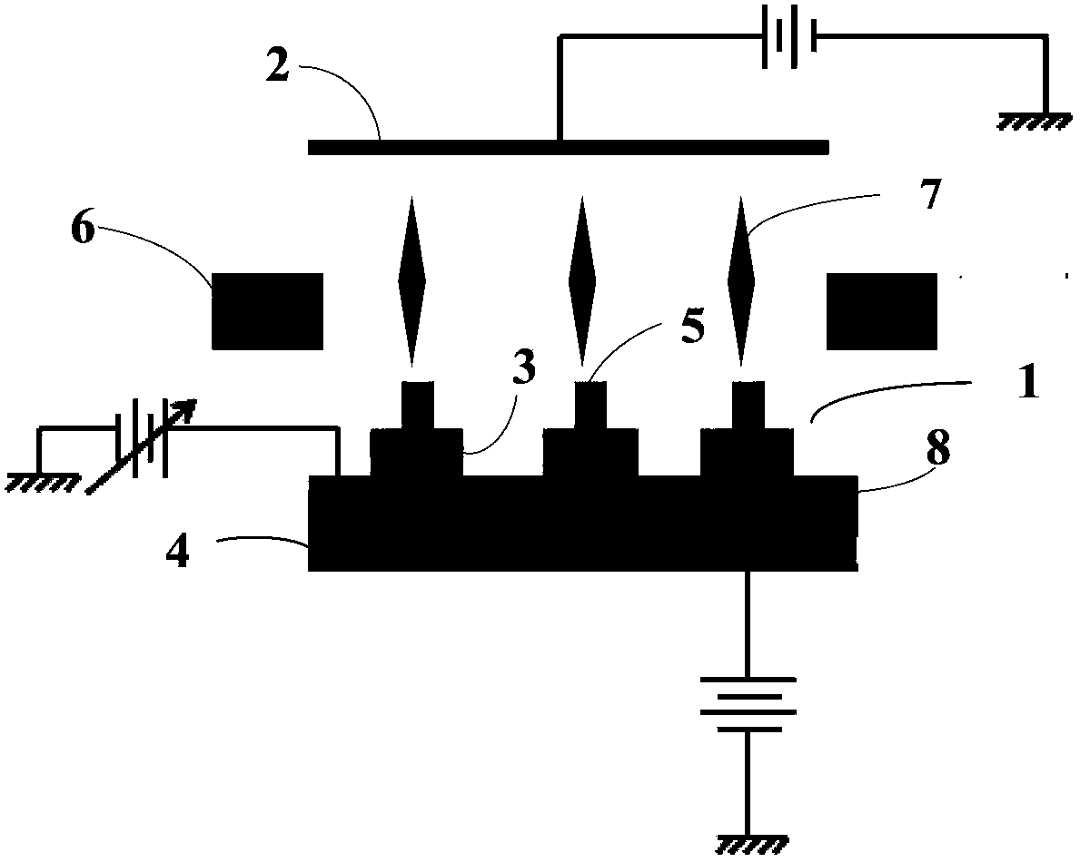
[0040] In order to solve the above technical problems, the present invention also provides a preparation method of a field emission electron source, Figure 9 It is a schematic diagram of the preparation process of the field emission electron source of the present invention. See Figure 9 , a method for preparing a field emission electron source, comprising the steps of:

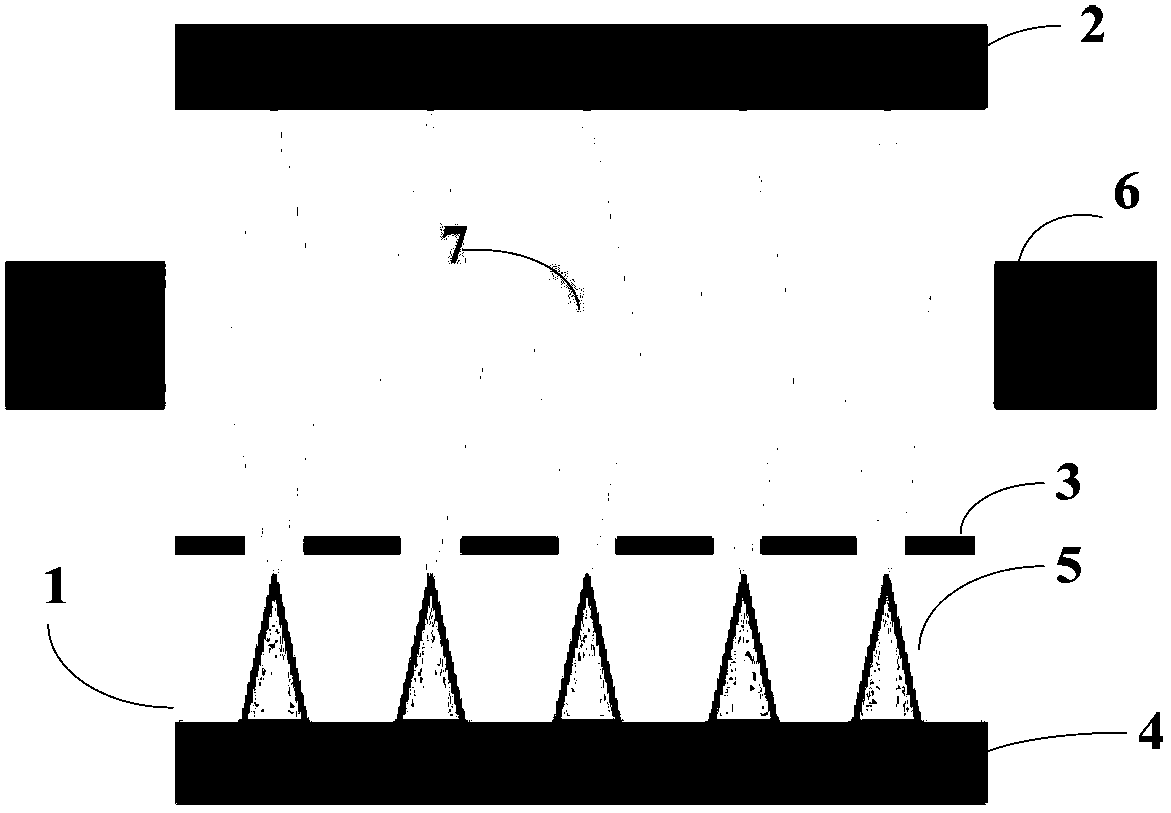
[0041] Executing step S10: etching the pretreated cathode substrate 4 to obtain a cathode 1 with an array of cathode emitters 5, the pretreatment method is: ultrasonically wash the cathode substrate 4 with deionized water and acetone for 1 to 3 Then dry at room temperature. The etching method may be photoetching, physical etching or chemical etching. In order to obtain nanometer or micron-scale array structure, chemical etching is preferred in the present invention.

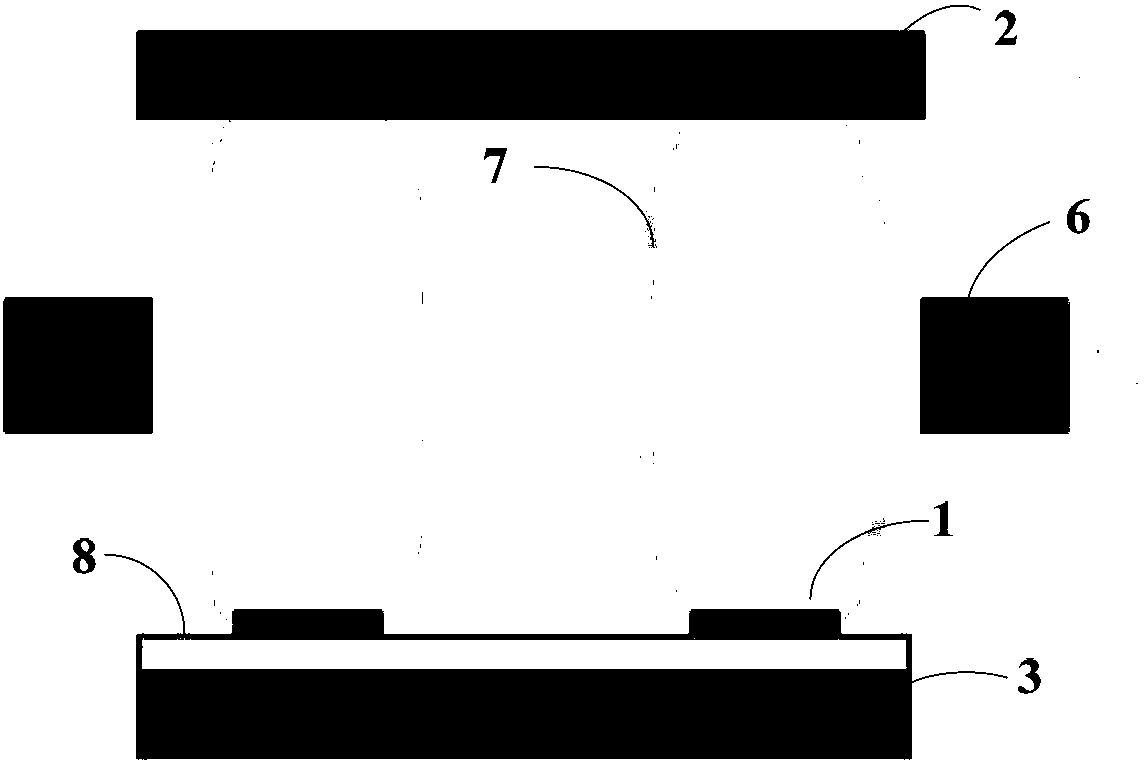
[0042] Executing step S20: depositing an insulating layer 8 on the surface of the cathode 1 having an array structure, for separating the c...

Embodiment 1

[0046] a) Take a heavily doped n-Si sheet as the cathode substrate, wash it ultrasonically for 1-3 times with deionized water and acetone respectively, and dry the obtained silicon sheet at room temperature for use.

[0047] b) Spin-coat photoresist on the surface of the silicon wafer, cover it with a mask plate, wash off the photoresist after one exposure to ultraviolet light, and obtain a surface patterned channel; use hydrogen fluoride (HF) to etch the Si wafer, and then protect it in an inert atmosphere The remaining photoresist was removed under high temperature to obtain a cathode Si sheet with an array structure, the height of the cathode base was 1 mm, and the height of the cathode emitter array was 100 μm.

[0048] c) Using chemical vapor deposition to deposit SiO on the cathode Si sheet with an array structure 2 insulating layer, the SiO 2 The height of the insulating layer is 80nm, continue to use the CVD method on the insulating layer SiO 2 Metal tungsten is depo...

Embodiment 2

[0051] a) Take a heavily doped n-Si wafer, wash it ultrasonically for 1-3 times with deionized water and acetone respectively, and dry the silicon wafer at room temperature for use.

[0052] b) Spin-coat photoresist on the surface of the silicon wafer, cover the mask plate with square gaps, wash off the photoresist after one exposure to ultraviolet light, and obtain a surface patterned channel; use HF to etch the Si wafer, and then under the protection of an inert atmosphere The remaining photoresist was removed at high temperature to obtain an etched Si sheet, the height of the cathode base was 2 mm, and the height of the cathode emitter array was 20 μm.

[0053] c) Spin-coat the photoresist on the etched Si wafer again, align the photolithographic template and the silicon wafer substrate on the positioning workbench, and wash off the photoresist after secondary ultraviolet exposure.

[0054] d) Depositing SiO on the surface of metal nanoarrays using ALD method 2 The insulat...


PUM


Abstract

The invention provides a field emission electron source which comprises a cathode, a grid electrode, an insulating layer and an anode opposite to the cathode, wherein the cathode comprises a cathode base and a cathode emitter array etched on the cathode base; and the grid electrode is arranged on the upper surface of the cathode base and on the side surface of any cathode emitter in the cathode emitter array by intervals of the insulating layer. The invention further provides a preparation method of the field emission electron source. The preparation method comprises the steps of etching to obtain the cathode emitter array on the surface of the cathode base, depositing the insulating layer on the surface of the patterned cathode, depositing the grid electrode on the surface of the insulating layer, etching on the surface of the grid electrode and on the insulating layer around the cathode emitters, exposing the cathode emitters, and obtaining the field emission electron source. The field emission electron source can improve the grid electron emissivity; the service life of the field emission electron source is prolonged; and the field emission electron source is simple in preparation technology, and is applicable to a cold cathode of an electron device.

Description

technical field [0001] The invention relates to the technical field of field emission, in particular to a field emission electron source and a preparation method thereof. Background technique [0002] As a device for emitting X-rays, X-ray vacuum tubes are widely used in medical, safety and industrial fields, such as X-ray imaging technology. The traditional X-ray generation mechanism is to emit high-energy thermal electrons to bombard the anode target by heating the cathode metal wire in the vacuum tube to generate X-rays. Compared with traditional thermionic emission, the field emission electron source does not need to be heated, and only needs to apply a certain electric field to generate a higher emission electron current density. Therefore, the field emission technology has gradually become an important electron emission technology due to its fast switching characteristics launch method. [0003] In the prior art, the field emission electron source mainly adopts a Spi...

Claims


Application Information

Patent Timeline
Patent Type & Authority Applications(China)
IPC IPC(8): H01J1/304H01J9/02
Inventor 李冬松章健
Owner SHANGHAI UNITED IMAGING HEALTHCARE
Why Eureka
Try Eureka