Micro-nano optical switch based on surface plasmon fano resonance and cascading optical switch using same
A surface plasmon and Fano resonance technology, which is applied in optics, nonlinear optics, instruments, etc., can solve the problem of non-wavelength selectivity and achieve the effect of simple preparation
- Summary
- Abstract
- Description
- Claims
- Application Information
AI Technical Summary
Problems solved by technology
Method used
Image
Examples
Embodiment 1
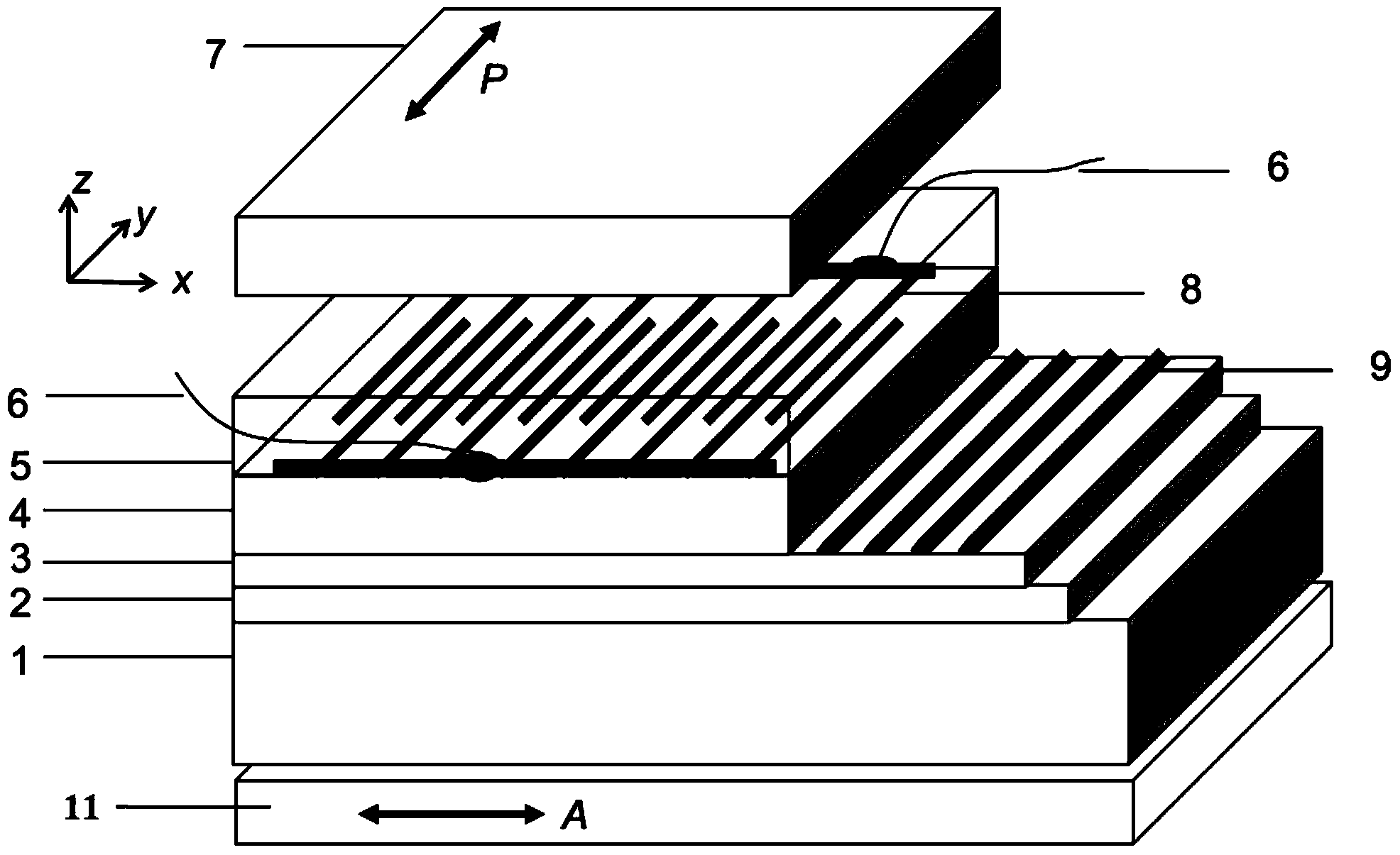
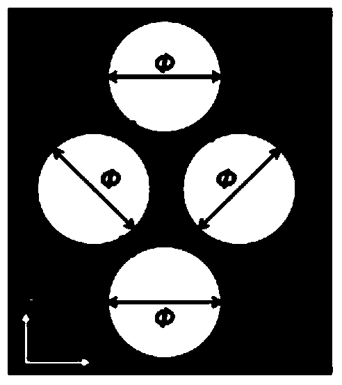
[0043] Embodiment 1: as figure 1 Shown is a specific embodiment of a micro-nano optical switch based on surface plasmon Fano resonance provided by the present invention, which adopts a glass transparent substrate, and a metal thin film layer 2 is stacked on the glass transparent substrate 1 in sequence , a nematic liquid crystal orientation switching layer and a polarizer 7, the nematic liquid crystal orientation switching layer in the present invention is composed of a polyimide film layer 3 and a nematic liquid crystal layer 4 successively stacked on the metal film layer 2 And the cover glass layer 5 constitutes. The upper surface of the polyimide film layer 3 is provided with several grooves 9 distributed in parallel at intervals, and the lower surface of the cover glass layer 5 is provided with interdigitated electrodes 8 and lead electrode lines 6, the interdigitated electrodes The interdigitation direction of 8 is parallel to the groove 9 below. In the present inventio...
Embodiment 2
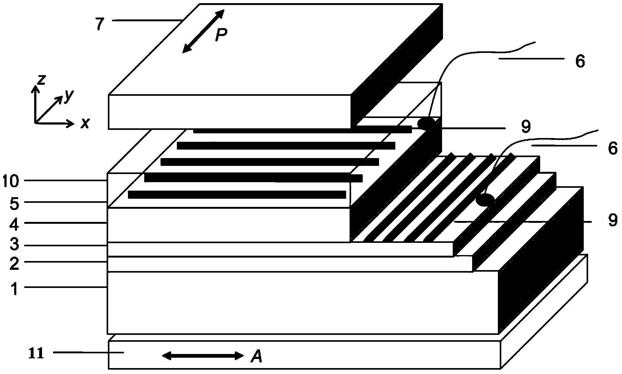
[0061] Embodiment 2: as figure 2 Shown is a specific embodiment of a micro-nano optical switch based on surface plasmon Fano resonance provided by the present invention, which adopts a glass transparent substrate, and a metal thin film layer 2 is stacked on the glass transparent substrate 1 in sequence , a nematic liquid crystal orientation switching layer and a polarizer 7, the nematic liquid crystal orientation switching layer in the present invention is composed of a polyimide film layer 3 and a nematic liquid crystal layer 4 successively stacked on the metal film layer 2 and ITO conductive film layer 10. Wherein the upper surface of polyimide thin film layer 3 is provided with some grooves 9 that are distributed in parallel at intervals, and the lower surface of ITO conductive film layer 10 is also provided with some grooves 9 that are distributed in parallel at intervals, these grooves 9 and polyimide The grooves 9 on the imide film layer 3 are vertical; in this embodim...
PUM
| Property | Measurement | Unit |
|---|---|---|
| thickness | aaaaa | aaaaa |
| pore size | aaaaa | aaaaa |
| diameter | aaaaa | aaaaa |
Abstract
Description
Claims
Application Information


