Organic light-emitting device and preparation method thereof

An electroluminescent device and luminescence technology, which is applied in the direction of electric solid-state devices, semiconductor/solid-state device manufacturing, electrical components, etc., can solve the problems of low light-emitting performance and total reflection loss of light-emitting devices, and achieve improved photon utilization and enhanced photon utilization. Reflective, stable effects

Inactive Publication Date: 2014-10-29
OCEANS KING LIGHTING SCI&TECH CO LTD +2
View PDF5 Cites 3 Cited by
  • Summary
  • Abstract
  • Description
  • Claims
  • Application Information

AI Technical Summary

Problems solved by technology

[0003] In a traditional light-emitting device, only about 18% of the light inside the device can be emitted to the outside of the device, while the rest will be consumed outside the device in other forms. This is due to the difference in refractive index between the interfaces (such as glass and The difference in refractive index between ITO, the refractive index of glass is 1.5, and ITO is 1.8, and the light from ITO to the glass will undergo total reflection), which causes the loss of total reflection, resulting in a lower overall light output performance of the light-emitting device

Method used


Image

  • Organic light-emitting device and preparation method thereof
  • Organic light-emitting device and preparation method thereof

Examples


Embodiment 1

[0054] A method for preparing an organic electroluminescent device, comprising the following steps:

[0055] (1) Wash the glass substrate with detergent, deionized water, and ultrasonic for 15 minutes to remove organic pollutants on the glass surface;

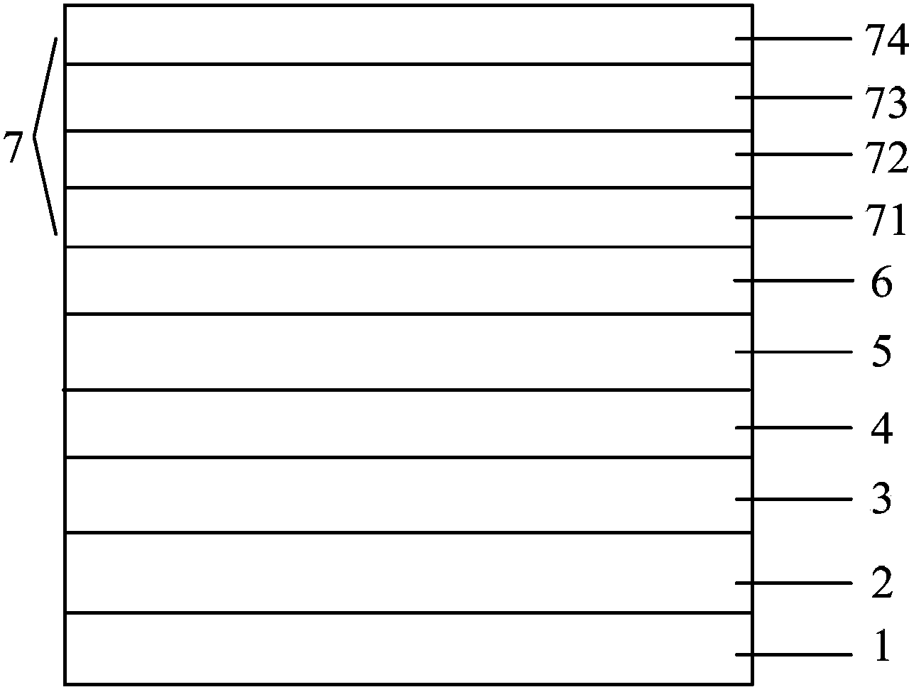
[0056] (2) Hole injection layer, hole transport layer, light-emitting layer, electron transport layer and electron injection layer were sequentially prepared on the ITO glass substrate by vacuum evaporation method;

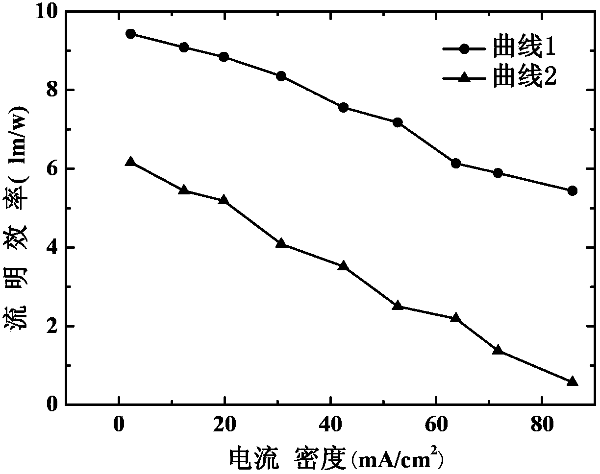
[0057] The evaporation of the hole injection layer, the hole transport layer, the light emitting layer, the electron transport layer and the electron injection layer is vacuum evaporation, the evaporation temperature is 400 ° C, and the vacuum degree is 1 × 10 -5 Pa. Wherein, the material of the hole injection layer is MoO 3 , the thickness is 30nm; the material of the hole transport layer is NPB, the thickness is 50nm; the material of the light-emitting layer is Alq 3 , the thickness of the light-emitting layer...

Embodiment 2

[0062] A method for preparing an organic electroluminescent device, comprising the following steps:

[0063] (1) Wash the glass substrate with detergent, deionized water, and ultrasonic for 15 minutes to remove organic pollutants on the glass surface;

[0064] (2) Hole injection layer, hole transport layer, light-emitting layer, electron transport layer and electron injection layer were sequentially prepared on the AZO glass substrate by vacuum evaporation method;

[0065] The evaporation of the hole injection layer, the hole transport layer, the light emitting layer, the electron transport layer and the electron injection layer is vacuum evaporation, the evaporation temperature is 400°C, and the vacuum degree is 1×10 -5 Pa. Wherein, the material of the hole injection layer is MoO 3 , with a thickness of 80nm; the material of the hole transport layer is TCTA, with a thickness of 60nm; the material of the light-emitting layer is ADN, with a thickness of 5nm; the material of t...

Embodiment 3

[0070] A method for preparing an organic electroluminescent device, comprising the following steps:

[0071] (1) Wash the glass substrate with detergent, deionized water, and ultrasonic for 15 minutes to remove organic pollutants on the glass surface;

[0072] (2) Hole injection layer, hole transport layer, light-emitting layer, electron transport layer and electron injection layer were sequentially prepared on the IZO glass substrate by vacuum evaporation method;

[0073] The evaporation of the hole injection layer, the hole transport layer, the light emitting layer, the electron transport layer and the electron injection layer is vacuum evaporation, the evaporation temperature is 400°C, and the vacuum degree is 1×10 -5 Pa. Wherein, the material of the hole injection layer is V 2 o 5 , the thickness is 20nm; the material of the hole transport layer is TCTA, the thickness is 30nm; the material of the light-emitting layer is Alq 3 , with a thickness of 40nm; the material of...


PUM

PropertyMeasurementUnit
glass transition temperatureaaaaaaaaaa
thicknessaaaaaaaaaa
thicknessaaaaaaaaaa

Abstract

The invention provides an organic light-emitting device comprising a conductive anode substrate, a hole injection layer, a hole transport layer, a luminescent layer, an electron transport layer, an electron injection layer and a composite cathode layer. The above-mentioned layers are successively laminated. The composite electrode layer consists of a zinc compound layer, an organic material layer, a metal layer and a passivation layer, wherein the layers are successively laminated. The zinc compound layer is made of a material from zinc oxide, zinc sulfide, zinc selenide, or zinc chloride; the organic material layer is made of an organic material with the highest occupied molecular orbital (HOMO) energy level of -6.5eV to -7.5eV and the glass-transition temperature of 50 to 100 DEG C; the metal layer is made of silver, aluminum, platinum or gold; and the passivation layer is made from silicon dioxide, aluminium oxide, or copper oxide. Because of the composite cathode layer, the light can be scattered and then be emitted to the bottom of the device, thereby improving the luminous efficiency of the device. In addition, the invention also provides a preparation method of the organic light-emitting device.

Description

technical field [0001] The invention relates to an organic electroluminescent device, in particular to an organic electroluminescent device and a preparation method thereof. Background technique [0002] In 1987, C.W.Tang and Van Slyke of Eastman Kodak Company in the United States reported a breakthrough in the research of organic electroluminescence. A high-brightness, high-efficiency double-layer organic electroluminescent device (OLED) has been prepared using ultra-thin film technology. In this double-layer structure device, the brightness reaches 1000cd / m at 10V 2 , its luminous efficiency is 1.51lm / W, and its lifespan is more than 100 hours. [0003] In a traditional light-emitting device, only about 18% of the light inside the device can be emitted to the outside of the device, while the rest will be consumed outside the device in other forms. This is due to the difference in refractive index between the interfaces (such as glass and The difference in refractive ind...

Claims


Application Information

Patent Timeline
Patent Type & Authority Applications(China)
IPC IPC(8): H01L51/52H01L51/54H01L51/56
CPCH10K50/826H10K50/854H10K50/856
Inventor 周明杰黄辉张振华王平
Owner OCEANS KING LIGHTING SCI&TECH CO LTD
Why Eureka
Try Eureka