

Novel two-sided thin film solar cell and industrial manufacturing method thereof
A thin-film solar cell and solar cell technology, which is applied in semiconductor/solid-state device manufacturing, circuits, photovoltaic power generation, etc., can solve the problems of low photoelectric conversion efficiency and increase battery costs, so as to improve photoelectric conversion efficiency, reduce device costs, and reduce cost effect
- Summary
- Abstract
- Description
- Claims
- Application Information
AI Technical Summary
Problems solved by technology
Method used
Image

Examples
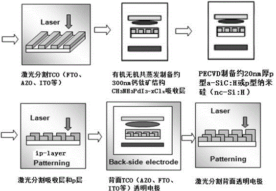
Embodiment 1
[0024] 1. The atomic layer deposition (ALD) method was used to prepare dense TiO with a thickness of 35nm on the FTO conductive glass 2 film;
[0025] 2. Then anneal at 450°C for 30 minutes;
[0026] 3. Vacuum deposition of 300nm ABX at a substrate temperature of 80°C and a pressure of 10Pa 3 Organic-inorganic hybrid perovskite absorber layer;
[0027] 4. PECVD deposition of p-type hydrogenated silicon thin film interface layer under the conditions of Table 2;
[0028] Substrate temperature (°C) RF power density (mW / cm 2 ) air pressure (Pa) H dilution ratio (H 2 / SiH 4 ) Deposition time (min) doping concentration p-Si:H 50-100 100-1000 100-1000 50,100,150 1-5 0.5%BF 3
[0029] 5. PECVD deposition p under the conditions of Table 3 + Hydrogenated silicon thin film heavily doped layer;
[0030] Substrate temperature (°C) RF power density (mW / cm 2 ) air pressure (Pa) H dilution ratio (H 2 / SiH 4 ) Depositi...
Embodiment 2
[0033] 1. Use FTO glass as the substrate for laser etching and cleaning;
[0034] 2. Prepare a dense ZnO film with a thickness of 35nm by sputtering;
[0035] 3. Anneal the ZnO film at 450°C for 30 minutes;
[0036] 4. Vacuum deposition of 300nm ABX under the conditions of substrate temperature of 80°C and pressure of 10Pa 3 Organic-inorganic hybrid perovskite absorber layer;
[0037] 5. PECVD deposition of p-type hydrogenated silicon carbon film interface layer under the conditions of Table 4;
[0038] Table 4 PECVD preparation conditions of p-SiC:H back electric field hole conduction layer
[0039]
[0040] 6. PECVD deposition of p+ hydrogenated silicon carbon thin film heavily doped layer under the conditions of Table 5;
[0041] Substrate temperature (°C) RF power density (mW / cm 2 ) air pressure (Pa) H dilution ratio (H 2 / SiH 4 ) Deposition time (min) doping concentration p-SiC:H 50-150 100-1000 100-1000 50,100,150 1-5 1.5%TM...
Embodiment 3
[0044] 1. Using ZnO glass as the substrate;
[0045] 2. Vacuum deposition of 300nm ABX under the conditions of substrate temperature of 80°C and pressure of 10Pa 3 Organic-inorganic hybrid perovskite absorber layer;
[0046] 3. PECVD deposition of p-type hydrogenated silicon carbon film interface layer under the conditions of Table 6;
[0047] Substrate temperature (°C) RF power density (mW / cm 2 ) air pressure (Pa) H dilution ratio (H 2 / SiH 4 ) Deposition time (min) doping concentration p-SiC:H 50-150 100-1000 100-1000 50,100,150 1-5 0.5%TMB
[0048] 4. PECVD deposition of p+ hydrogenated silicon carbon thin film heavily doped layer under the conditions of Table 7;
[0049] Table 7p + -PECVD Preparation Conditions of SiC:H Hole Conducting Layer in Back Electric Field
[0050]
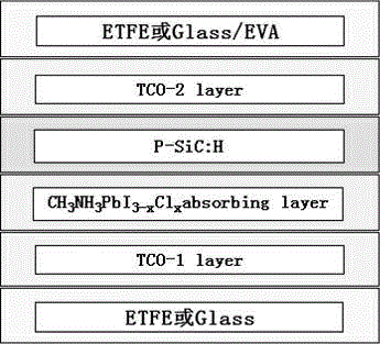
[0051] 5. Use the magnetron sputtering coating system to sputter on the surface of the p-layer silicon film to prepare the ITO transparent conductive ...
PUM
 Abstract
Description
Claims
Application Information