Unlock instant, AI-driven research and patent intelligence for your innovation.

Transparent conductive electrode and preparation method thereof, and OLED display device

A technology for transparent conductive electrodes and display devices, which is applied in electric solid devices, semiconductor devices, organic semiconductor devices, etc., can solve the problem that transparent conductive electrodes cannot simultaneously integrate conductivity, light transmittance and ductility.

Active Publication Date: 2014-12-03
BOE TECH GRP CO LTD
View PDF2 Cites 2 Cited by
  • Summary
  • Abstract
  • Description
  • Claims
  • Application Information

AI Technical Summary

Problems solved by technology

[0005] Embodiments of the present invention provide a transparent conductive electrode and its preparation method, and an OLED display device, which can solve the problem that the transparent conductive electrode cannot simultaneously integrate conductivity, light transmittance and ductility in the prior art

Method used


Image

  • Transparent conductive electrode and preparation method thereof, and OLED display device
  • Transparent conductive electrode and preparation method thereof, and OLED display device
  • Transparent conductive electrode and preparation method thereof, and OLED display device

Examples


preparation example Construction

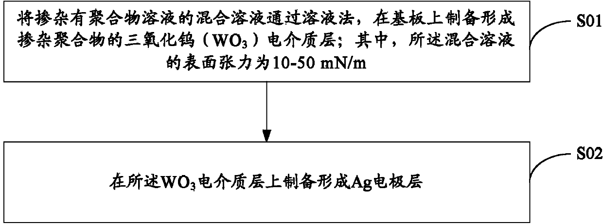
[0039] Embodiments of the present invention provide a method for preparing a transparent conductive electrode, such as figure 1 As shown, the method includes the following steps:

[0040] S01, the mixed solution doped with polymer solution is prepared on the substrate to form tungsten trioxide (WO) doped polymer by solution method 3 ) dielectric layer; wherein, the surface tension of the mixed solution is 10-50mN / m.

[0041] Here, due to the final preparation of WO doped with the polymer through the above mixed solution 3 Dielectric layer, therefore, in the mixed solution, besides including the polymer solution, it should also include the 3 solution, such as tungstic acid solution.

[0042] On this basis, a solution method was used to prepare WO 3 The dielectric layer is: the above mixed solution is coated on the substrate, for example, by spin coating, and then the WO doped with the polymer is formed through a related process. 3 Dielectric.

[0043] Wherein, due to the ...

Embodiment 1

[0066] Example 1, a 7nm Ag electrode layer was prepared by vacuum thermal evaporation, the surface roughness Rq was measured with an atomic force microscope (AFM), the surface resistance was measured with a four-probe method, and the transmittance was tested with an optical transmittance tester. rate, the test results are shown in the first row of Table 1.

Embodiment 2

[0067] Embodiment two, Na 2 WO 4 The aqueous solution is passed through the strong acid cation exchange resin to obtain H 2 WO 4 Solution, 10mL concentration of 1mol / L H 2 WO 4 The solution was coated on the substrate by spin coating, and after baking at 200°C for 1 hour, a 20nm WO 3 Dielectric layer, and finally prepare a 10nm Ag electrode layer by vacuum thermal evaporation; use an atomic force microscope to test the surface roughness Rq, use the four-probe method to test the surface resistance, and use an optical transmittance tester to test the transmittance. The test results are shown in the second row of Table 1.


PUM

PropertyMeasurementUnit
surface tensionaaaaaaaaaa
thicknessaaaaaaaaaa
thicknessaaaaaaaaaa

Abstract

The invention provides a transparent conductive electrode and a preparation method thereof, and an OLED display device, relates to the field of display technology, and aims at solving the problems that the conductivity, the light transmittance and the ductility of a transparent conductive electrode in the prior art cannot be synthesized at the same time. The preparation method of the transparent conductive electrode comprises that a tungsten trioxide dielectric layer doped with a polymer is prepared on a substrate from a mixed solution doped with a polymer solution by a solution method, and the surface tension of the mixed solution is 10 to 50 mN / m; and an Ag electrode layer is prepared on the tungsten trioxide dielectric layer. The method is applied to preparation of the transparent conductive electrode and the OLED display device.

Description

technical field [0001] The invention relates to the field of display technology, in particular to a transparent conductive electrode, a preparation method thereof, and an OLED display device. Background technique [0002] Indium Tin Oxide (ITO for short) has conductivity and transparency, so it is the most commonly used film material for transparent conductive electrodes. Taking Organic Light Emitting Diode (OLED) display devices as an example, traditional OLED display devices use ITO electrodes and metal electrodes (such as: silver, magnesium, aluminum, etc.) as the anode and cathode of the device, and the anode and cathode There is an organic material functional layer in between, and the luminescence of the device can be observed from the transparent ITO side, and the metal cathode acts as a reflective layer. [0003] However, although ITO has relatively good light transmittance (>90%), its application also has many limitations, such as: a) relatively poor electrical c...

Claims


Application Information

Patent Timeline
Patent Type & Authority Applications(China)
IPC IPC(8): H01L51/56H01L51/52
CPCH10K2102/00H10K71/441H10K71/60H10K77/111H10K59/805
Inventor 尤娟娟
Owner BOE TECH GRP CO LTD
Features
  • R&D
  • Intellectual Property
  • Life Sciences
  • Materials
  • Tech Scout
  • Unparalleled Data Quality
  • Higher Quality Content
  • 60% Fewer Hallucinations
Learn More