Dielectric composite material for fingerprint sensor induction layer and preparation method thereof

A fingerprint sensor and composite material technology, applied in the direction of acquiring/organizing fingerprints/palmprints, circuits, electrical components, etc., can solve problems such as low efficiency, high manufacturing cost, and complicated sensor packaging process

Active Publication Date: 2014-12-10
TECORE SYNCHEM
View PDF11 Cites 38 Cited by
  • Summary
  • Abstract
  • Description
  • Claims
  • Application Information

AI Technical Summary

Problems solved by technology

[0006] In addition to the IC encapsulation process, the lens-encapsulated fingerprint sensor needs additional encapsulation processes such as pre-cutting and pasting of the capacitive lens, which makes the sensor encapsulation process particularly complicated, and thus its manufacturing cost is high
[0007] In short, the existing technologies for encapsulating silicon wafers all require complex encapsulation manufacturing processes, which are costly and inefficient

Method used


Image

  • Dielectric composite material for fingerprint sensor induction layer and preparation method thereof
  • Dielectric composite material for fingerprint sensor induction layer and preparation method thereof
  • Dielectric composite material for fingerprint sensor induction layer and preparation method thereof

Examples


Embodiment 1-1

[0091] Preparation of Dielectric Composite Materials for Sensing Layer of Fingerprint Sensor

[0092] Small batch preparation method:

[0093] (1) take by weighing raw material according to embodiment 1;

[0094] (2) Mix the epoxy resin, the inorganic filler of the first type of dielectric, the inorganic filler of the second type of dielectric and the adhesion promoter at 150°C for 0.5 hours through a double-roller rubber mixer, and then add Release agent and flame retardant, knead for 1 minute; adjust the temperature to 80°C, add phenolic resin and catalyst, knead for 10 minutes until uniform, extrude into thin flakes, cool to room temperature, crush and make cakes to obtain The dielectric composite material used in the sensing layer of the fingerprint sensor is stored in a sub-zero refrigerator for future use.

[0095] Above-mentioned process parameter is the same as embodiment 1-1 in table 2.

[0096] Example 1-1 in Table 2, the number "1" before the "-" in "1-1" refers to...

Embodiment 40

[0103] The use of dielectric composite materials for the sensing layer of fingerprint sensors:

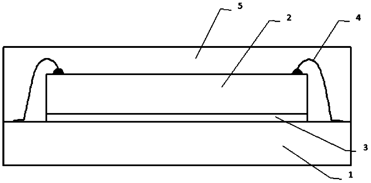
[0104] The dielectric composite material used for the sensing layer of the fingerprint sensor is covered on the fingerprint sensor chip by high-temperature molding injection molding (hydraulic method), and the dielectric composite material used for the sensing layer of the fingerprint sensor is completely cured by heating and curing, so that The fingerprint sensor chip can sense the electrical signal on the fingerprint, and finally recognize different fingerprint patterns, so it can be used very well on the fingerprint sensor (see figure 1 ).

[0105] figure 1 Among them, 1 is the packaging substrate; 2 is the sensor chip; 3 is the chip bonding material; 4 is the bonding wire; 5 is the dielectric composite material used in the fingerprint sensor sensing layer of the present invention.

Embodiment 41

[0107] Table 3. Properties of Dielectric Composite Materials Used in Sensing Layers of Fingerprint Sensors

[0108]

[0109]

[0110] The maximum particle size of the first and second types of dielectric inorganic fillers used in the sensing layer of the fingerprint sensor is <100 μm, and the average particle size is between 0.8 μm and 50 μm. When the dielectric composite materials are used in combination, the helical flow length of the dielectric composite material in the sensing layer of the prepared fingerprint sensor is longer and the flow effect is better.

[0111] Table 4. Encapsulation properties of dielectric composites for sensing layers of fingerprint sensors

[0112]

[0113]

[0114] The thickness of the dielectric composite material of the sensing layer of the fingerprint sensor is 200 μm, the curing condition is 170° C., and the curing time is 200 seconds. The composite materials prepared in Examples 5, 8, 10, 13, 16, 20, 24, 26, 28 and 37 have a har...


PUM

PropertyMeasurementUnit
thicknessaaaaaaaaaa
thicknessaaaaaaaaaa
thicknessaaaaaaaaaa

Abstract

The invention discloses a dielectric composite material for a fingerprint sensor induction layer and a preparation method thereof. The dielectric composite material is prepared from an epoxy resin, a phenol aldehyde resin, a first dielectric inorganic filler, a second dielectric inorganic filler, a curing agent, an adhesion accelerator, a releasing agent and a flame retardant. The dielectric composite material has the advantages of high dielectric constant, small dielectric loss, stable dielectric properties (can not greatly change along with test frequency), non-transparency and high hardness; and the prepared fingerprint sensor induction layer satisfies the requirements for reliability and stability on the premise of achieving the thickness requirement, and can be used in various portable electronic products. The dielectric composite material is free of heavy metal lead, and thus, is green and environment-friendly. The dielectric composite material is convenient and safe; and thus, the terminal not only can be substituted for the existing digital-input cryptographic identification system, and can also be used on any electronic component in need of privacy.

Description

technical field [0001] The invention relates to a dielectric composite material used for the sensing layer of a fingerprint sensor and a preparation method. Background technique [0002] The packaging structure of a typical fingerprint sensor currently includes a silicon wafer on which sensing electrodes and related circuits are formed. The function of the fingerprint sensor (Finger Print Sensor, FPS for short) is to sense the relative distance between the ridge (Ridge, that is, the raised pattern) and the valley (Valley, that is, the concave pattern) of the skin of the user's finger in the capacitive electric field, and generate an accurate fingerprint. and valley texture image. In order to ensure the accuracy of the sensor, the distance between the user's finger and the surface of the silicon wafer should not be too large; when the distance between the finger and the surface of the silicon wafer increases, the electric field strength decreases, the sensing accuracy of the...

Claims


Application Information

Patent Timeline
Patent Type & Authority Applications(China)
IPC IPC(8): C08L63/00C08L61/06C08K13/02C08K3/24C08K3/22C08K3/36C08K3/38C08K3/26C08K3/34
CPCC04B26/14C04B2111/92C04B24/302C04B14/305C04B14/06C04B24/121C04B24/42C04B24/36C04B22/06C04B14/327C04B22/066C04B14/28C04B24/2611C04B22/064C08L61/06C08G59/50C08G59/621B29C48/001B29C48/022C08L63/00H01L2224/48465H01L2224/48091H01L2224/73265H01L2224/32225H01L2924/181H01L2224/48227G06V40/1329G06V40/1306C08K3/22C08K5/0066C08K5/54H01L2924/00014H01L2924/00012H01L2924/00B29K2061/04B29K2063/00B29K2105/0026B29K2509/00B29K2995/0006B29K2995/0016C08L2201/02
Inventor 谭晓华霍钜于会云冯亚凯孙绪筠
Owner TECORE SYNCHEM
Why Eureka
Try Eureka