Amorphous semiconductor film and preparation method and application thereof

A technology of amorphous semiconductor and thin film, which is applied in semiconductor/solid-state device manufacturing, semiconductor devices, transistors, etc., can solve the problems of limited storage, achieve small sub-threshold swing, wide application prospects, and improve the effect of TFT driving ability

Inactive Publication Date: 2014-12-17
PEKING UNIV
View PDF6 Cites 14 Cited by
  • Summary
  • Abstract
  • Description
  • Claims
  • Application Information

AI Technical Summary

Problems solved by technology

However, due to the extremely limited reserves of indium (In) in the world, IGZO is only a temporary choice, and other oxide semiconductor materials must be developed to replace IGZO

Method used


Image

  • Amorphous semiconductor film and preparation method and application thereof
  • Amorphous semiconductor film and preparation method and application thereof
  • Amorphous semiconductor film and preparation method and application thereof

Examples


Embodiment Construction

[0031] Below in conjunction with the accompanying drawings of the description, the present invention will be further described by examples.

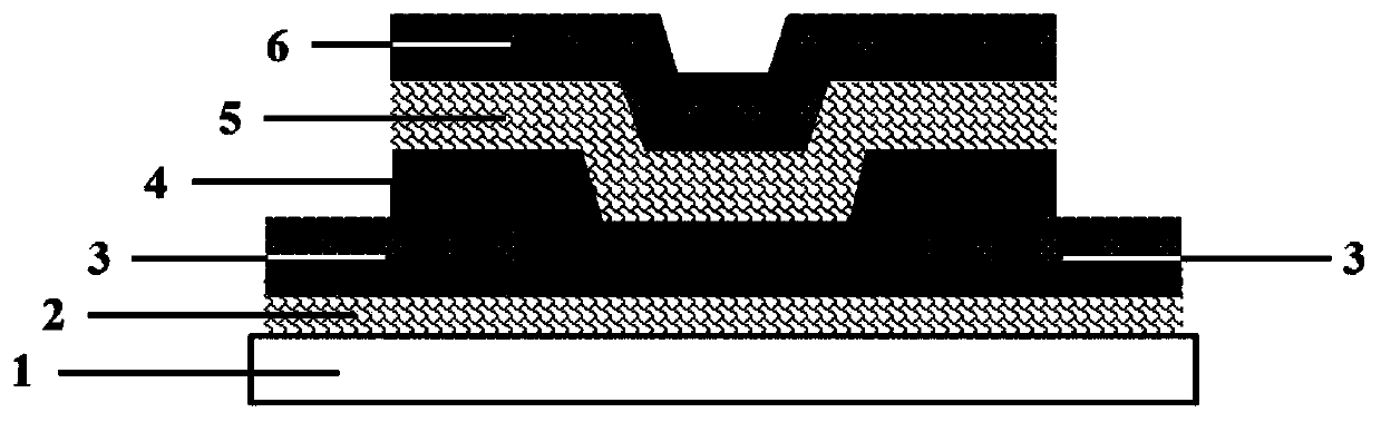
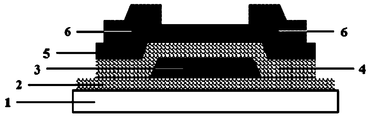
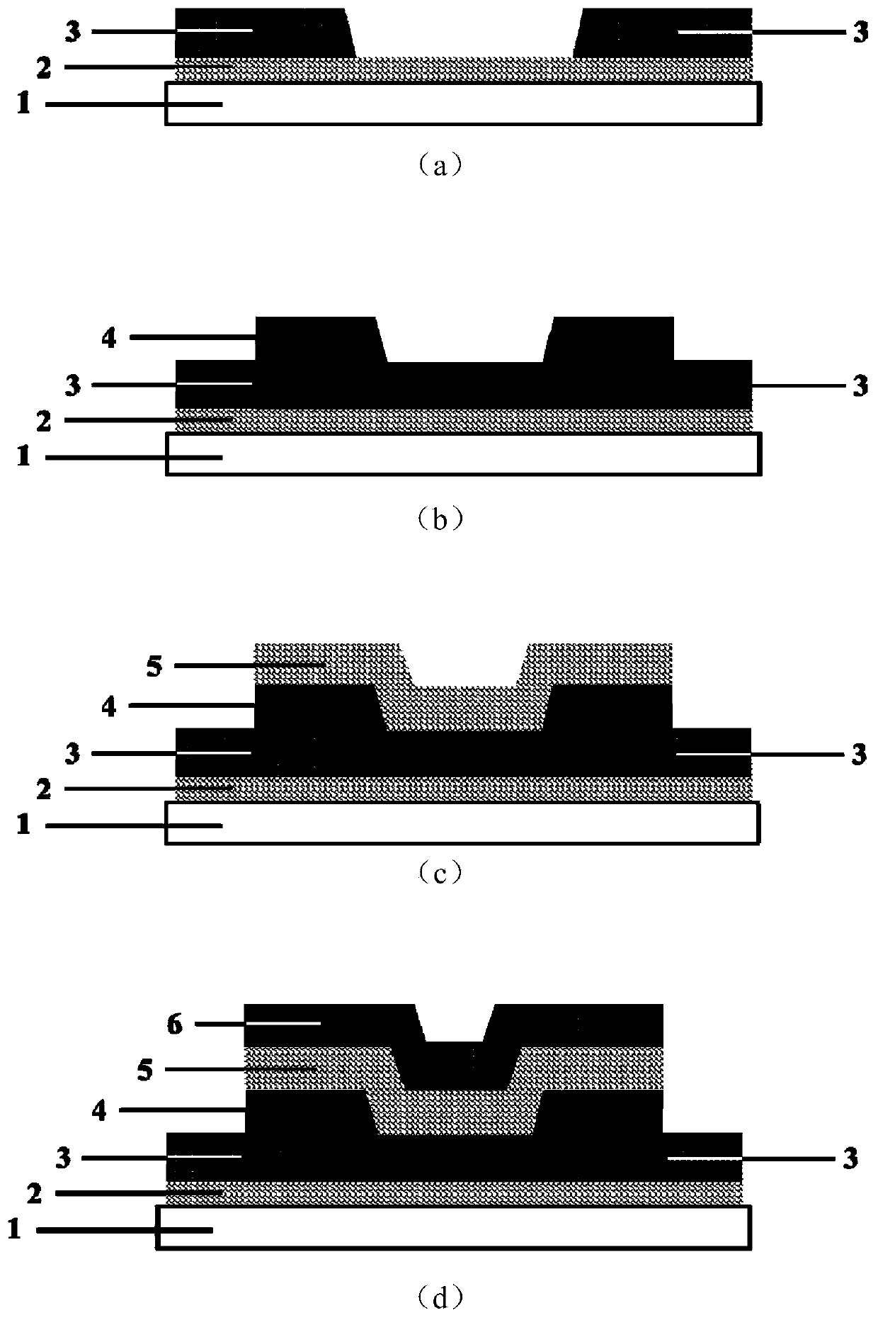
[0032] The amorphous zinc-aluminum oxide film doped with rare earth elements provided by the present invention is formed on the surface of a semiconductor or glass substrate by a sputtering method, and the molar percentage content of zinc, aluminum and rare earth elements in the semiconductor film is: zinc element 85%- 98%, aluminum element 1%-10%, rare earth element 1%-14%, rare earth element is at least one of Gd, Lu, Y and Sc.

[0033] figure 1 The illustrated thin film transistor includes a source electrode and a drain electrode, an active region, a gate dielectric layer, and a gate electrode. The source and drain electrodes are located on the substrate, the active region is located on the substrate and the source and drain electrodes, the gate dielectric layer is located on the active region, and the gate electrode is located on th...


PUM

PropertyMeasurementUnit
thicknessaaaaaaaaaa

Abstract

The invention discloses an aluminum zinc oxide amorphous semiconductor film material and a preparation method and application thereof and belongs to the technical field of semiconductor integrated circuits and manufacture thereof. The amorphous semiconductor film comprises, by mole percent content, 85-98% of zinc element, 1-10% of aluminum element and 1-14% of rare earth element, wherein the rare earth element is at least one of Gd, Lu, Y and Sc. A radio frequency magnetron sputtering method is adopted to prepare the aluminum zinc oxide film material doped with the rare earth element, the voltage division ratio of oxygen atmosphere is adjusted in the sputtering process to form a channel material which has amorphous characteristics and is high in migration rate. The preparation method is compatible with a traditional complementary metal oxide semiconductor (CMOS) process, and a rare earth doped oxide semiconductor film transistor can be prepared, is high in practical value and can be applied to future thin film transistor (TFT) integrated circuits.

Description

technical field [0001] The invention belongs to the field of integrated circuit manufacturing and flat panel display, and in particular relates to an oxide film material doped with rare earth elements and a preparation method thereof. Background technique [0002] With the development of integrated circuit manufacturing and flat panel display technology, it is extremely important to improve the performance of thin film transistors (TFT) and reduce its production cost to promote the development of flat panel display. In recent years, the technology of oxide semiconductor TFTs, especially Indium Gallium Tin Oxide (IGZO)-TFT, has developed rapidly, and has already possessed the capability of mass production. Display products with IGZO-TFT as the basic unit are just around the corner. However, due to the extremely limited reserves of indium (In) in the world, IGZO is only a temporary choice, and other oxide semiconductor materials must be developed to replace IGZO. [0003] Alu...

Claims


Application Information

Patent Timeline
Patent Type & Authority Applications(China)
IPC IPC(8): H01L29/24H01L29/04H01L21/363H01L21/443H01L29/786H01L21/34
CPCH01L21/02565H01L29/66742H01L29/78693
Inventor 王漪韩德栋董俊辰赵飞龙丛瑛瑛张翼张盛东刘力锋刘晓彦康晋锋
Owner PEKING UNIV
Why Eureka
Try Eureka