Organic monolayer thin film field effect gas sensor and preparation method thereof

A technology of gas sensor and thin film field effect, which is applied in the direction of instruments, scientific instruments, analytical materials, etc. It can solve the problems of inability to achieve high response efficiency and long response time of sensors

Active Publication Date: 2015-01-21
THE NAT CENT FOR NANOSCI & TECH NCNST OF CHINA
View PDF5 Cites 16 Cited by
  • Summary
  • Abstract
  • Description
  • Claims
  • Application Information

AI Technical Summary

Problems solved by technology

[0006] But, above-mentioned gas sensor based on organic field effect tube also has its weak point
For example, when the traditional active layer with a thickness of tens of nanometers is used for gas detection, because most of the gas molecules are distributed on the surface of the active layer, and the conductive channels involved in carrier transport in the active layer are located closest to

Method used


Image

  • Organic monolayer thin film field effect gas sensor and preparation method thereof
  • Organic monolayer thin film field effect gas sensor and preparation method thereof
  • Organic monolayer thin film field effect gas sensor and preparation method thereof

Examples


preparation example Construction

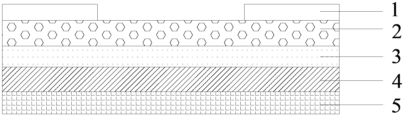
[0044] A preparation method of the gas sensor, the preparation method adopts a vacuum evaporation method to evaporate an organic monomolecular thin film layer on the dielectric layer 3; during evaporation, the evaporation source is first heated to a target temperature (such as 123°C ), after the deposition rate is stable, turn on the beam baffle to start evaporation; the evaporation rate is selected appropriately (such as 1.5nm / min), the purpose is to ensure that the evaporated molecular layer grows in a two-dimensional growth mode, and control the evaporation time (such as 1min) to obtain an organic monomolecular thin film layer as the active layer 2.

[0045] The metal foil used as the source-drain electrode 1 is directly attached to the surface of the organic monomolecular film layer by mechanical means.

[0046] Specifically, a preparation such as figure 2 The main process of the organic monolayer thin film field-effect gas sensor shown is as follows:

[0047] (1) In Si / S...

specific Embodiment 1

[0052] Select the Si / SiO2 sheet purchased from Hefei Kejing Material Technology Co., Ltd. as the substrate, cut it into a size of about 1×1cm, use acetone, ethanol, and deionized water to clean it ultrasonically for 10 minutes, and then use a hot stage at 100°C Bake for 2h. Spin coating after drying. The spin coating process is completed on the laurell WS-400MZ-8NPP-LITE spin coater. The substrate is adsorbed on the spin coater, and the speed is set at 6000 / min. The solution is dropped on the surface of the substrate, the solution is required to cover the substrate, and the spin coating is started. After the spin coating is completed, the sample is placed in a vacuum drying oven, and the baking temperature is set to 85° C., and baked for 12 hours.

[0053] After the sample is dried, the key step of evaporation of the organic active layer is carried out. This process is completed on the auto306 vacuum evaporation equipment of BOC-Edwards Company. After loading the crucible wi...

specific Embodiment 2

[0056] Specific embodiment 2 (comparative example)

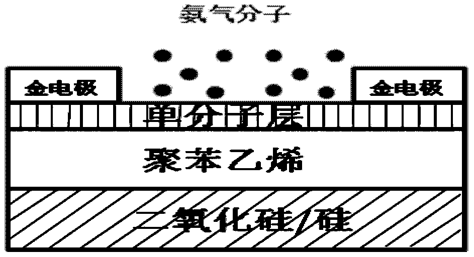
[0057] A field-effect gas sensor with an organic active layer thickness of 40 nm was prepared. The preparation method was described in Example 1, except that the vapor deposition time of pentacene was appropriately prolonged to obtain an active layer with a film thickness of 40 nm. The prepared 40nm thick film sensor is tested for ammonia molecules, and the test results are compared with the test results of the monomolecular layer sensor in Example 2. The specific comparison method is: source and drain of the two sensors in different concentrations of ammonia gas Changes in current are compared. It is found that the source-drain current of the monolayer sensor has a more obvious change with the concentration of ammonia gas, indicating that the monomolecular layer sensor has higher sensitivity than the thick film sensor. The whole test result is as Figure 5 .


PUM

PropertyMeasurementUnit
Thicknessaaaaaaaaaa
Thicknessaaaaaaaaaa
Thicknessaaaaaaaaaa

Abstract

The present invention relates to an organic monomolecular layer thin film field effect gas sensor and a preparing method of the same. The forming structure of the gas sensor includes a substrate, a gate electrode, a dielectric layer, an active layer and a source-drain electrode from bottom to top, and the active layer is an organic monomolecular thin film layer. In the preparing method, an organic monomolecular thin film layer is evaporated on a dielectric layer by using a vacuum evaporation method; during evaporation, first an evaporating source is heated to a target temperature (such as 123°C), and after the deposition rate is stable, a beam baffle is opened to begin evaporation; evaporation time is controlled to obtain an organic monomolecular thin film layer serving as an active layer. According to the technical solution of the present invention, by means of a gas sensor with a pentacene monomolecular layer serving as an active layer, all pentacene molecules in the active layer can contact the outside world. When the sensor is working, pentacene molecules interact with detected gas directly without obstruction, and this interaction can be sensitively reflected in a change of an output curve of a thin film transistor thereof.

Description

technical field [0001] The invention relates to the technical field of gas sensors, in particular to an organic monomolecular layer thin film field-effect gas sensor and a preparation method. Background technique [0002] Organic thin film transistor (OTFT), also known as organic field effect transistor, is a type of structure similar to traditional inorganic field effect transistor (FET), but the active layer is based on organic semiconductors (small molecules or polymers with conjugated π electron structures) New electronic devices. It has the advantages of light weight, simple preparation process, low price and compatibility with flexible substrates, so it has received widespread attention since its inception. At present, its performance is close to or exceeds the level of amorphous silicon thin film transistors, and is widely used in organic light-emitting display OLED drive, organic radio frequency tags and organic sensors and other fields. [0003] A sensor is a devi...

Claims


Application Information

Patent Timeline
IPC IPC(8): G01N27/414
CPCG01N27/4141
Inventor 江潮王嘉玮米斯巴·莫扎李德兴
Owner THE NAT CENT FOR NANOSCI & TECH NCNST OF CHINA
Why Eureka
Try Eureka