
Method for manufacturing thin film capacitor with anodic oxidation film as dielectric layer

An anodized film, film capacitor technology, applied in capacitor manufacturing, capacitors, circuits, etc., can solve the problems of complex production process of air bridge, complex equipment and process, poor film compactness, etc., to achieve capacitance value and withstand voltage value The effect of easy adjustment of size, good electrical properties, and low manufacturing cost

Active Publication Date: 2015-02-04
CHINA ELECTRONIS TECH INSTR CO LTD
View PDF5 Cites 6 Cited by
  • Summary
  • Abstract
  • Description
  • Claims
  • Application Information

AI Technical Summary

Problems solved by technology

The disadvantage of this manufacturing process is that in addition to physical vapor deposition coating equipment, large and expensive equipment such as plasma chemical vapor deposition and dry etching are required, and a complex manufacturing process for air bridges is required.
For example, it is mentioned in the published patent CN 1295341A: adopt low-pressure chemical vapor deposition (LPCVD) to obtain amorphous Ta 2 o 5 thin film, however this amorphous Ta 2 o 5 The compactness of the thin film is not good, it needs to undergo low temperature annealing and high temperature annealing in an annealing furnace with a certain gas atmosphere to make the amorphous Ta 2 o 5 Film crystallization and densification to improve leakage current characteristics and dielectric properties of film capacitors
It is not difficult to see from the patent description that this method requires complex equipment and processes, and the production process is cumbersome and costly

Method used


Image

  • Method for manufacturing thin film capacitor with anodic oxidation film as dielectric layer
  • Method for manufacturing thin film capacitor with anodic oxidation film as dielectric layer
  • Method for manufacturing thin film capacitor with anodic oxidation film as dielectric layer

Examples


Embodiment 1

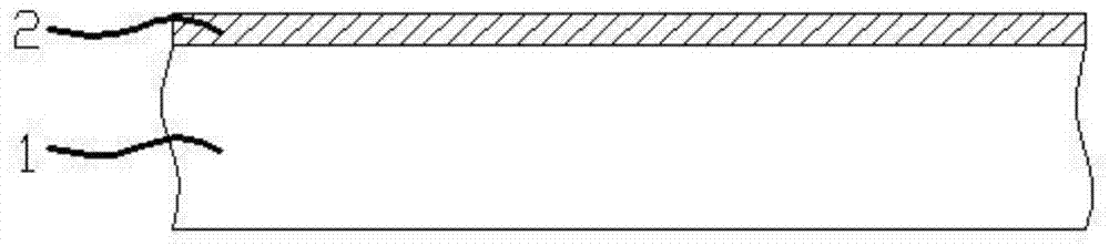
[0057] On a sapphire substrate 1 with a thickness of 0.254mm, a Ta film is deposited as a metal film 2 by magnetron sputtering, and the thickness of the Ta film is about 300nm, such as figure 1 shown.

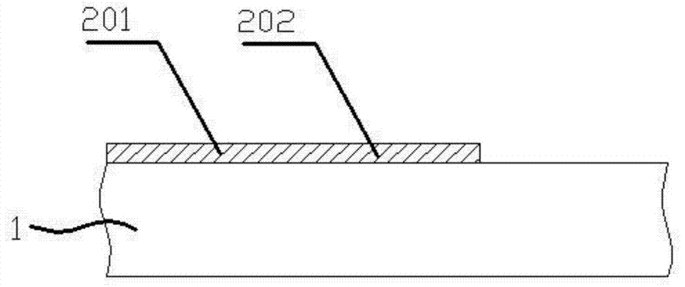
[0058] The metal thin film 2 is patterned by a photolithographic etching process to form the lower electrode 202 and the first lower electrode lead-out line 201, such as figure 2 shown. Among them, Ta corrosion solution uses HF buffer solution.

[0059] A photoresist was spin-coated on the bottom electrode 202 and the first bottom electrode lead-out line 201, and an anodic oxidation mask was formed by a photolithography process. The thickness of the patterned anodic oxidation mask 3 was 8 microns. The anodization mask 3 completely covers the first lower electrode lead-out lines 201 to prevent the first lower electrode lead-out lines 201 from being oxidized during anodization. The opening area of ​​the anodic oxidation mask 3 is larger than the lower electrode 202 so as to e...


PUM

PropertyMeasurementUnit
Thicknessaaaaaaaaaa
Thicknessaaaaaaaaaa

Abstract

The invention discloses a method for manufacturing a thin film capacitor with an anodic oxidation film as a dielectric layer. The method comprises the following steps: a substrate is prepared, and a layer of metal or metal oxide thin film is deposited on the substrate; the thin film is patterned by a photolithography and etching process to form a lower electrode and a first lower electrode lead-out wire; photoresist is applied to the lower electrode and the first lower electrode lead-out wire, and an anodic oxidation mask is formed through a photolithography process; anode oxidation is carried out on the lower electrode to form a dielectric layer; and the photoresist is removed, an electrode layer is deposited on the substrate, and the electrode layer is patterned by a photolithography and etching process to form a second lower electrode lead-out wire, an upper electrode, and an upper electrode lead-out wire. Manufacturing equipment and processes needed by the method are simple, the manufacturing cost is low, the capacitance value and voltage value are easy to adjust, and excellent electrical characteristics are achieved.

Description

technical field [0001] The invention relates to a method for manufacturing a film capacitor whose dielectric layer is an anodized film. Background technique [0002] The development trend of microwave electronic products and electronic complete machines is "light, thin, short, small", multi-functional, high assembly density and high reliability. Integrating metal transmission lines, resistors, capacitors, inductors and other components on the substrate is conducive to reducing the circuit volume, improving integration, reducing parasitic parameters, and improving circuit bandwidth and high-frequency characteristics. Among them, the integration of film capacitors on the substrate is a key technology, and the existing technologies include the following: [0003] Silicon nitride is used as the dielectric layer material of thin-film capacitors. Due to the residual stress of the sputtered silicon nitride film, the adhesion of the film layer is not good. The plasma-enhanced chemi...

Claims


Application Information

Patent Timeline
IPC IPC(8): H01G13/00
Inventor 宋振国王斌路波曹乾涛胡莹璐
Owner CHINA ELECTRONIS TECH INSTR CO LTD
Features
  • Generate Ideas
  • Intellectual Property
  • Life Sciences
  • Materials
  • Tech Scout
  • Unparalleled Data Quality
  • Higher Quality Content
  • 60% Fewer Hallucinations
Learn More