Method for manufacturing black silicon materials

A black silicon and silicon substrate technology, applied in the field of photoelectric sensitive materials, can solve the problems of black silicon material performance degradation, near-infrared light absorption rate decrease, black silicon material absorption decrease, etc.

Inactive Publication Date: 2015-02-11
UNIV OF ELECTRONICS SCI & TECH OF CHINA
View PDF4 Cites 3 Cited by
  • Summary
  • Abstract
  • Description
  • Claims
  • Application Information

AI Technical Summary

Problems solved by technology

But at the same time, crystalline silicon itself has its own inherent defects: First, the surface of crystalline silicon has a high reflection of visible-infrared light. If the expensive surface of the crystal is not treated, its reflectivity of visible-infrared light is above 30%. The reflection of ultraviolet light is as high as more than 50%; secondly, the band gap of crystalline silicon material is 1.124eV at room temperature (300K), which leads to a greatly reduced absorption rate of near-infrared light with a wavelength greater than 1100nm
[0008] Moreover, the black silicon material is obtained after processing on the basis of the silicon material, and its surface is forest-like pointed cones, pyramids or needles, which makes black silicon have large surface defects, and it is even more so after the introduction of doping. The photoelectric conversion performance of the material is reduced
Due to the uneven surface and many defects of black silicon materials, the dark current is relatively large. How to reduce the dark current of black silicon materials is an urgent problem to be solved.
[0009] The annealing process and surface passivation can reduce the surface defects of the black silicon material and reduce the dark current, but the impurities introduced by the femtosecond irradiation of the silicon material after annealing will diffuse to the grain boundaries of the silicon substrate, resulting in a decrease in the impurity concentration, resulting in The absorption of light by black silicon material decreases, which reduces the performance of black silicon material

Method used


Image

  • Method for manufacturing black silicon materials
  • Method for manufacturing black silicon materials
  • Method for manufacturing black silicon materials

Examples


Embodiment Construction

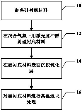
[0030] The specific steps of the method for manufacturing black silicon material according to the embodiment of the present invention will be described in detail below with reference to the accompanying drawings.

[0031] figure 1 It is a schematic flowchart of a method for manufacturing black silicon material according to an embodiment of the present invention. Such as figure 1 As shown, in this embodiment, the method for manufacturing black silicon material may include step 10 , step 12 , step 14 and step 16 . These steps will be described in detail below with reference to non-limiting specific examples.

[0032] Step 10: Prepare silicon substrate material.

[0033] In the embodiment of the present invention, the silicon substrate material is prepared first. The high infrared absorption silicon material of the embodiment of the present invention will be made based on the silicon substrate material.

[0034] In the embodiment of the present invention, the silicon substra...


PUM

PropertyMeasurementUnit
wavelengthaaaaaaaaaa
reflectanceaaaaaaaaaa

Abstract

The embodiment of the invention discloses a method for manufacturing black silicon materials. The method comprises the following steps that silicon substrate materials are prepared; the silicon substrate materials are illuminated by laser pulses in mixed atmosphere of nitrogen and sulfur hexafluoride; a passivation layer is deposited on the surface of the silicon substrate materials subjected to the laser pulse illumination; the silicon substrate materials subjected to the passivation layer deposition is subjected to high-temperature annealing treatment. According to the method provided by the embodiment of the invention, during the black silicon material manufacturing, the laser pulse is used for illumination in the mixed atmosphere of the nitrogen and the sulfur hexafluoride, then, the black silicon materials are formed through processes such as surface passivation layer deposition, the formed black silicon materials realize the absorption higher than 93 percent in the whole wave band being 350nm to 2500nm, in addition, the absorption rate after the high-temperature annealing treatment only generates a little vertical deflection, and the high absorption rate in the whole wave band is still maintained.

Description

[0001] technical field [0002] The invention relates to the technical field of photoelectric sensitive materials, in particular to a method for manufacturing black silicon materials. [0003] Background technique [0004] In the semiconductor industry, crystalline silicon materials are widely used in microelectronics, photovoltaic industry, communication and other fields due to their rich resources, easy acquisition, easy purification, easy doping, high temperature resistance and many other advantages. But at the same time, crystalline silicon itself has its own inherent defects: First, the surface of crystalline silicon has a high reflection of visible-infrared light. If the expensive surface of the crystal is not treated, its reflectivity of visible-infrared light is above 30%. The reflection of ultraviolet light is as high as more than 50%. Secondly, the band gap of crystalline silicon material is 1.124eV at room temperature (300K), which leads to a greatly reduced abso...

Claims


Application Information

Patent Timeline
Patent Type & Authority Applications(China)
IPC IPC(8): H01L31/18
CPCH01L31/1804H01L31/1864H01L31/1868Y02P70/50
Inventor 李世彬王健波杨光金黄俊龙吴志明
Owner UNIV OF ELECTRONICS SCI & TECH OF CHINA
Why Eureka
Try Eureka