Semiconductor starting device based on spiral polycrystalline silicon field effect transistor charging and manufacturing process of semiconductor starting device

A field effect transistor and spiral technology, which is applied in the field of integrated circuit start-up devices, can solve the problems affecting power conversion efficiency, heat dissipation and reliability, the resistance value of resistor R1 cannot be too large, and the size of switching power supply is large, so as to improve power supply efficiency. , Low power consumption, small chip area

Inactive Publication Date: 2015-02-18
CHENGDU SMET TECH
View PDF7 Cites 6 Cited by
  • Summary
  • Abstract
  • Description
  • Claims
  • Application Information

AI Technical Summary

Problems solved by technology

[0003] The defect of the above-mentioned traditional switching power supply start-up circuit is: when the input voltage Vin range is wide, in order to ensure that the control IC can provide enough power at the lowest input voltage Starting current, so that the switching power supply can start normally, then the resistance value of resistor R1 should not be too large
Since the resistor R1 is always connected to the input terminal, the power consumption generated by the resistor R1 is P=(Vin-VCC)2 / R1. Obviously, if the switching power supply is working at a high voltage input, the power consumption on the resistor R1 will be very high. If it is large, it will affect the power conversion efficiency, heat dissipation and reliability, and reduce the power supply efficiency. Moreover, the resistor R1 must use a high-power resistor, so that the switching power supply is large in size and high in cost.

Method used


Image

  • Semiconductor starting device based on spiral polycrystalline silicon field effect transistor charging and manufacturing process of semiconductor starting device
  • Semiconductor starting device based on spiral polycrystalline silicon field effect transistor charging and manufacturing process of semiconductor starting device
  • Semiconductor starting device based on spiral polycrystalline silicon field effect transistor charging and manufacturing process of semiconductor starting device

Examples


Embodiment Construction

[0024] The present invention will be further described below in conjunction with accompanying drawing:

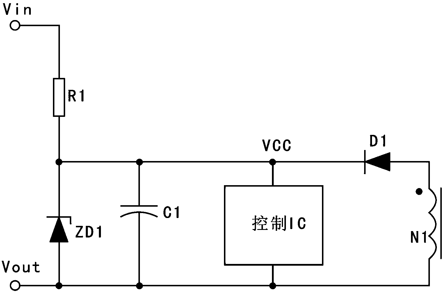
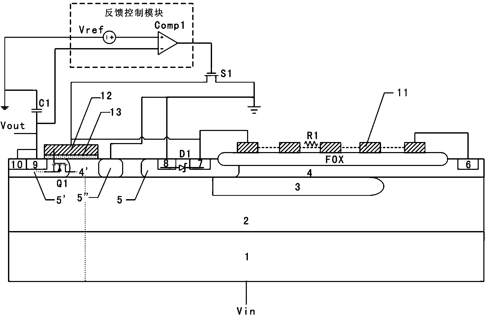
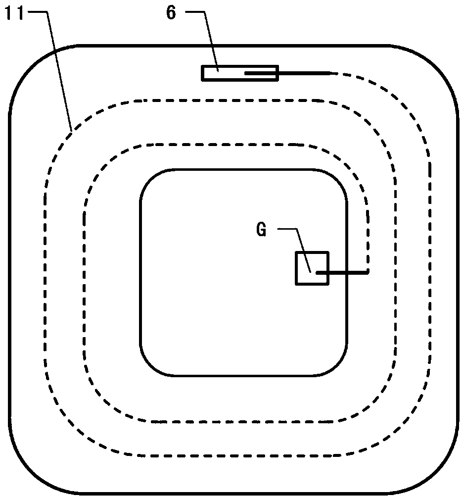
[0025] Such as figure 2 with image 3 as shown, figure 2 The power input terminal, power output terminal, resistor R1 and capacitor C1 are respectively connected with figure 1 Correspondingly, so adopted the same symbol; The semiconductor start-up device charged based on the spiral polysilicon type field effect tube of the present invention, the input voltage Vin of its power supply input is charged by capacitor C1, and the two ends of capacitor C1 are power output terminals, Its output voltage Vout supplies power to the main circuit (not shown in the figure), an N-type lightly doped epitaxial layer 2 is provided on the N-type high-concentration substrate 1, and a P type buried layer 3, a first N well 4 is arranged on the P type buried layer 3, a first N type heavily doped 6 and a thick oxide layer FOX are arranged on the first N well 4, and a spiral shape is arranged ...


PUM


Abstract

The invention discloses a semiconductor starting device based on spiral polycrystalline silicon field effect transistor charging. The semiconductor starting device is characterized in that the first end of a resistor is connected with the drain of a field effect transistor to serve as an input end, the second end of the resistor, the grid of the field effect transistor and the first end of an electronic switch are connected with the cathode of a diode, the source of the field effect transistor and the cathode signal input end of a feedback control module are connected with the first end of a capacitor to serve as an output end, the output end of the feedback control module is connected with the control input end of the electronic switch, and the anode signal input end of the feedback control module, the second end of the capacitor, the second end of the electronic switch and the anode of a voltage stabilizing diode are grounded. The invention further discloses a manufacturing process of the semiconductor starting device. The manufacturing process uses the field effect transistor integrated by a BCD process, the resistor and the voltage stabilizing diode. The semiconductor starting device has the advantages that the integrated field effect transistor is used to directly charge the capacitor, and due to the fact the integrated field effect transistor is low in resistance and power consumption when the field effect transistor is on, high power efficiency, low loss and low heating value are achieved.

Description

technical field [0001] The invention relates to an integrated circuit starting device, in particular to a semiconductor starting device and a manufacturing process based on charging of a spiral polysilicon type field effect transistor. Background technique [0002] The switching power supply starting circuit is a commonly used starting device in integrated circuits. At present, the structure (or basic principle) of most switching power supply starting circuits is as follows: figure 1 As shown, it includes resistor R1, capacitor C1, Zener diode ZD1, auxiliary winding N1, diode D1 and control IC. The current is greater than the starting current of the control IC. After the voltage of the capacitor C1 rises to the normal operating voltage of the control IC, the control IC starts to work. When the output voltage Vout of the starting circuit is stable, the voltage generated by the auxiliary winding N1 is rectified by the diode D1 and the capacitor C1 supplies power to the contro...

Claims


Application Information

Patent Timeline
Patent Type & Authority Applications(China)
IPC IPC(8): H01L27/06H02M1/36H01L21/822
Inventor 胡浩
Owner CHENGDU SMET TECH
Why Eureka
Try Eureka