Metal electrode patch production method
A metal electrode and patch technology, applied in the electrical field, can solve the problems of film solution damage, complex process, low yield, etc., and achieve the effect of reducing bonding force, high conductivity and small thickness
- Summary
- Abstract
- Description
- Claims
- Application Information
AI Technical Summary
Problems solved by technology
Method used
Image
Examples
Embodiment 1
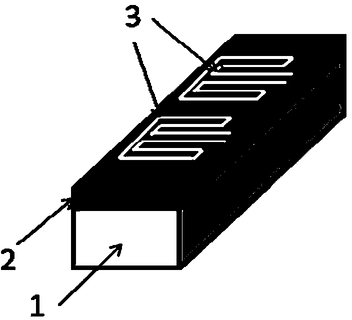
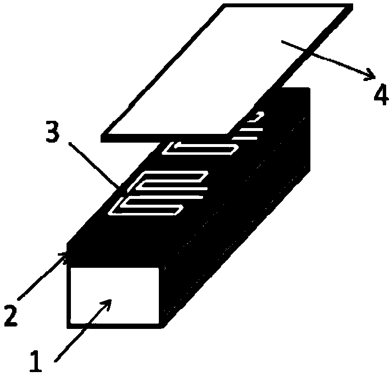
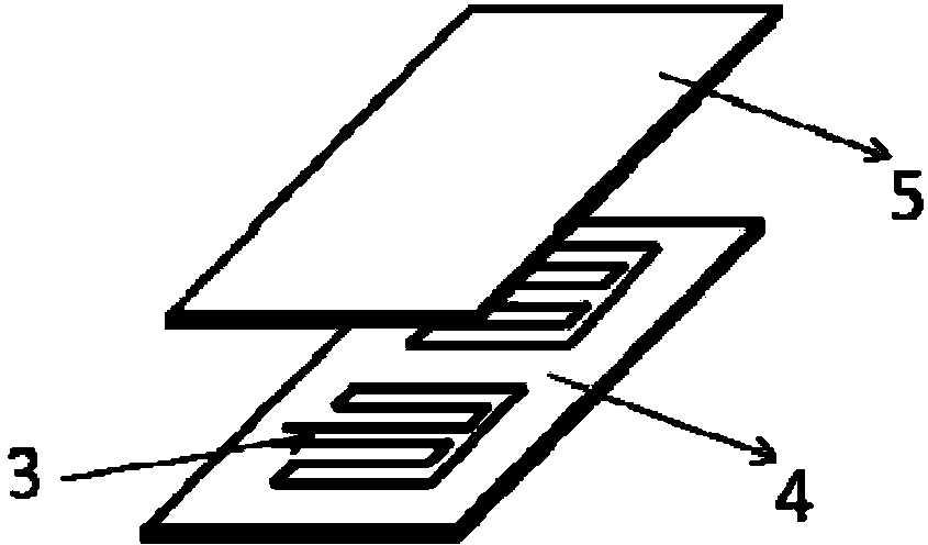
[0035] Embodiment 1 and comparative example 1 refer to attached Figure 1~4 , in combination with the content of the invention, the embodiments of the present invention will be described in detail.
[0036] Example 1
[0037] Step 1 selects a polysilicon wafer as a supporting substrate. Such as figure 1 As shown, a polysilicon wafer 1 for solar cells is used, and a layer of silicon nitride film is grown on it by PECVD after polishing with a mixture of hydrofluoric acid and nitric acid. The thickness of the silicon nitride film is 100 nm, and then The surface of the silicon nitride film is made hydrophilic by irradiating the surface with ozone for 10 minutes with ultraviolet light.
[0038] Step 2 Printing of electrodes: Use screen printing technology to print silver paste 3 on the surface of the substrate silicon nitride film 2 after the above treatment according to the required electrode pattern, and multiple electrode patterns can be printed at one time; the printing thic...
Embodiment 2
[0049] Embodiment 2 refers to the appended Figure 1~4 , in combination with the content of the invention, the embodiments of the present invention will be described in detail.
[0050] Step 1 Preparation of ceramic support substrate: as figure 1 As shown, a silicon dioxide ceramic substrate 1 is used, the surface is polished into a mirror surface, and a layer of silicon nitride film is grown on it by PECVD method. Here, the thickness of the silicon nitride film is 100nm, and then the surface is treated with ultraviolet light for 10 minutes by irradiating ozone. Make the surface of the silicon nitride film hydrophilic.
[0051] Step 2 Printing of electrodes: Use screen printing technology to print silver paste 3 on the surface of the substrate silicon nitride film 2 after the above treatment according to the required electrode pattern, and multiple coils can be printed at one time; the printing thickness of silver paste is about 35 Micron, the silver content in the silver pa...
Embodiment 3
[0057] A method for preparing a metal electrode patch with high conductivity, comprising the following steps:
[0058] Using high-temperature-resistant nitride silicon nitride ceramics, the surface of silicon nitride ceramics is firstly polished to Ra<0.01, and then the surface of ozone is treated with hydrophilicity, and the silver paste is printed on the surface treated or coated according to the required electrode pattern. On the support substrate, the support substrate printed with the electrode paste is dried at 150°C-220°C, cooled to room temperature, and then sintered at 1200°C at a high temperature; after cooling, the sintered metal electrode is separated from the Glue it off the support substrate, and then paste it on the protective film to form an electrode patch.
PUM
| Property | Measurement | Unit |
|---|---|---|
| thickness | aaaaa | aaaaa |
| thickness | aaaaa | aaaaa |
| thickness | aaaaa | aaaaa |
Abstract
Description
Claims
Application Information
 - R&D
- Intellectual Property
- Life Sciences
- Materials
- Tech Scout
- Unparalleled Data Quality
- Higher Quality Content
- 60% Fewer Hallucinations
Browse by: Latest US Patents, China's latest patents, Technical Efficacy Thesaurus, Application Domain, Technology Topic, Popular Technical Reports.
© 2025 PatSnap. All rights reserved.Legal|Privacy policy|Modern Slavery Act Transparency Statement|Sitemap|About US| Contact US: help@patsnap.com


