
Epitaxial slice of GaN-based light emitting diode (LED) and preparation method thereof

A technology of light-emitting diodes and epitaxial wafers, applied in electrical components, circuits, semiconductor devices, etc., can solve problems such as high V-type and defects, and achieve the effect of reducing the number, delaying V-type defects, and improving crystal quality and antistatic ability.

Inactive Publication Date: 2015-02-18
HC SEMITEK SUZHOU
View PDF4 Cites 28 Cited by
  • Summary
  • Abstract
  • Description
  • Claims
  • Application Information

AI Technical Summary

Problems solved by technology

[0006] In order to solve the problem of V-shaped defects introduced in the stress release layer with high In content grown under low temperature and constant temperature conditions in the prior art, an embodiment of the present invention provides an epitaxial wafer of a GaN-based light-emitting diode and its preparation method

Method used


Image

  • Epitaxial slice of GaN-based light emitting diode (LED) and preparation method thereof
  • Epitaxial slice of GaN-based light emitting diode (LED) and preparation method thereof

Examples


Embodiment 1

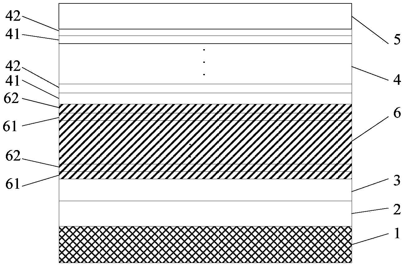
[0027] An embodiment of the present invention provides an epitaxial wafer of a GaN-based light emitting diode, see figure 1 , the epitaxial wafer comprises a substrate 1, a buffer layer 2 grown on the substrate 1, an N-type layer 3, a multi-quantum well layer 4 and a P-type layer 5, the multi-quantum well layer 4 is a superlattice structure, and the multi-quantum well Each cycle of layer 4 includes In y Ga 1-y N layer 41 and GaN layer 42, 0x Ga 1-x N layer 61 and grown on In x Ga 1-x For the GaN layer 62 on the N layer 61, 0x Ga 1-x The content of In in the N layer 61 increases layer by layer with the number of periods.

[0028] In this embodiment, the number of periods of the stress release layer 6 may be 2-20.

[0029] When implemented, the multi-quantum well layer 4 is directly grown on the last GaN layer 62 in the stress release layer 6 . Since the composition of the GaN layer is relatively simple and the growth quality is better, the multi-quantum well layer grown ...

Embodiment 2

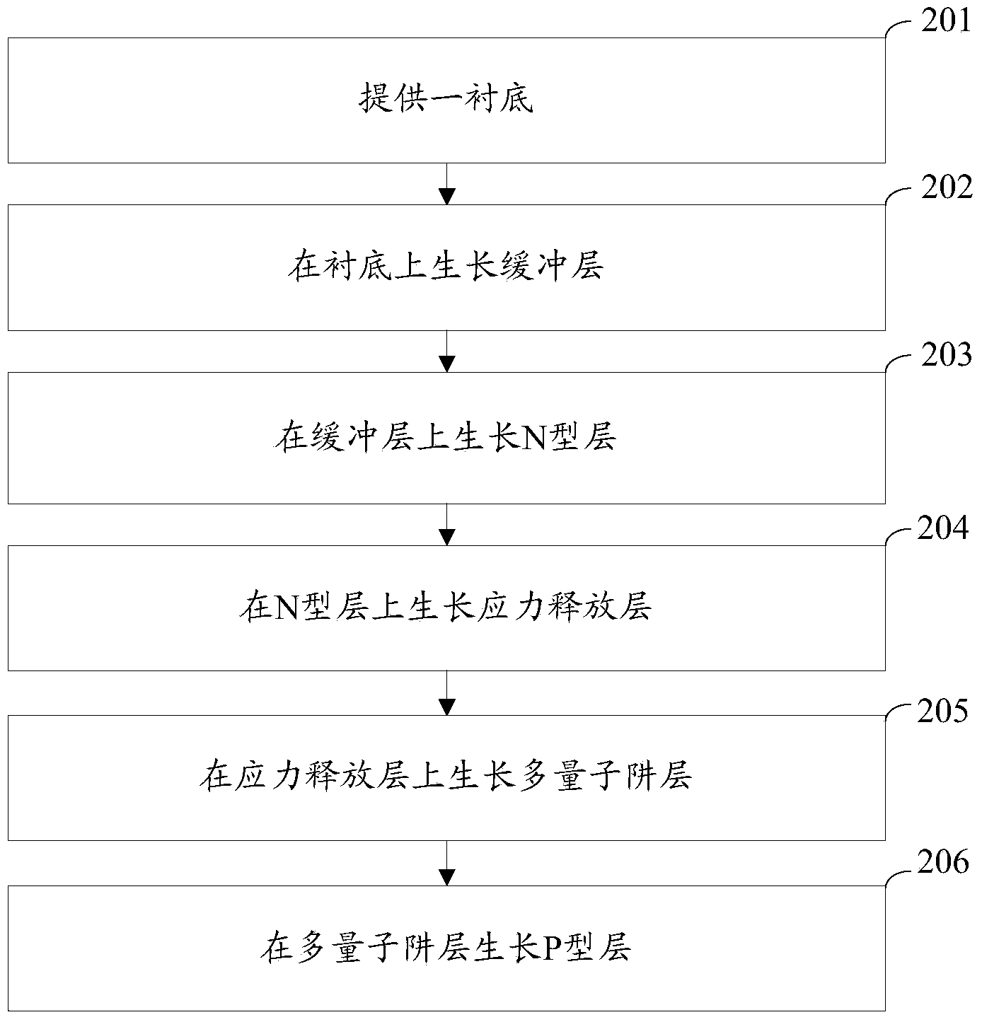
[0045] An embodiment of the present invention provides a method for preparing an epitaxial wafer of a GaN-based light-emitting diode, see figure 2 , the method includes:

[0046] Step 201: Provide a substrate.

[0047] Specifically, the substrate may be a sapphire substrate, and may also be a Si substrate or a SiC substrate.

[0048] This step may also include cleaning the surface of the substrate. When it is realized, the sapphire substrate can be heated to 1110°C in a MOCVD (Metal-organic Chemical Vapor Deposition) reaction chamber, under hydrogen (H 2 ) atmosphere for annealing and nitriding the sapphire substrate for 8-10 minutes to clean the surface of the substrate.

[0049] Step 202: growing a buffer layer on the substrate.

[0050] Wherein, the buffer layer may be a composite layer, which may include a low-temperature buffer layer and an undoped GaN layer. Specifically, at a temperature of 540° C., a GaN layer with a thickness of 30 nm is grown on the substrate a...


PUM

PropertyMeasurementUnit
Growth temperatureaaaaaaaaaa
Growth thicknessaaaaaaaaaa
Electron concentrationaaaaaaaaaa

Abstract

The invention discloses an epitaxial slice of a GaN-based light emitting diode (LED) and a preparation method thereof, and belongs to the LED field. The preparation method of the epitaxial slice of the GaN-based LED includes a step of sequentially growing a buffer layer, an N type layer, a stress release layer, a multiple quantum well layer and a P type layer on a substrate, wherein each period of the multiple quantum well layer comprises an InyGa1-y N layer and a GaN layer, the stress release layer is of a super lattice structure, each period of the stress release layer comprises an InxGa1-x N layer and another GaN layer, y is larger than x, x is larger than 0, growth temperature of the stress release layer is gradually reduced along with periodicity change from the N type layer, and the content of In of each InxGa1-x N layer is increased layer by layer along with the periodicity change. The preparation method of the epitaxial slice of the GaN-based LED effectively delays growth of V-shaped defects by using the temperature varying and In content varying stress release layer and arranging a high temperature and low In content growth stress release layer on one side of the epitaxial slice of the GaN-based LED, close to the N type layer, and thereby effectively reduces the quantity of the V-shaped defects, improves crystalline quality of the multiple quantum well layer, and then improves inner quantum efficiency and antistatic ability of the GaN-based LED.

Description

technical field [0001] The invention relates to the field of light-emitting diodes, in particular to an epitaxial wafer of a GaN-based light-emitting diode and a preparation method thereof. Background technique [0002] In the development of the LED (Light Emitting Diode, light-emitting diode) industry, GaN, a semiconductor material with a wide bandgap (Eg>2.3eV), has developed extremely rapidly, and GaN-based LEDs have been commercialized very quickly. [0003] The epitaxial wafer of a traditional GaN-based light-emitting diode includes a sapphire substrate, a buffer layer grown sequentially on the sapphire substrate, an undoped GaN layer, an N-type layer, a multi-quantum well layer and a P-type layer. Wherein, the multi-quantum well layer is a superlattice structure, and each period includes alternately grown InGaN layers and GaN layers. Due to the large lattice mismatch between InGaN and GaN, the crystal quality is poor, and leakage current is easy to form, and there ...

Claims


Application Information

Patent Timeline
IPC IPC(8): H01L33/12H01L33/32H01L33/00
CPCH01L33/12H01L33/005H01L33/32H01L33/325
Inventor 乔楠李昱桦韩杰胡加辉魏世祯
Owner HC SEMITEK SUZHOU
Learn More