Low-input capacitance power semiconductor field effect transistor and self-alignment manufacture method thereof
A technology of field effect transistors and power semiconductors, applied in semiconductor/solid-state device manufacturing, semiconductor devices, circuits, etc., can solve the problems of device switching speed reduction, increase switching power loss, and reduce circuit efficiency, so as to reduce input capacitance and improve Effect of switching speed and shortening switching time
- Summary
- Abstract
- Description
- Claims
- Application Information
AI Technical Summary
Problems solved by technology
Method used
Image

Examples
Embodiment approach 1
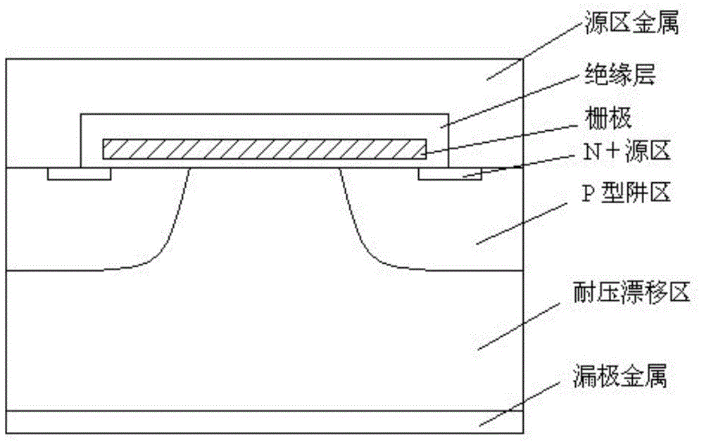
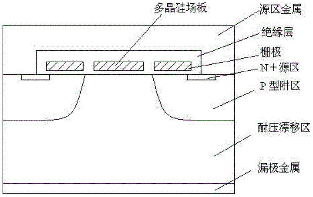
[0026] Take the VDMOSFET device as an example, such as figure 2 As shown, the polysilicon gate of the existing device is disconnected at the edge of the JFET region, and is divided into the polysilicon gate of the device and the polysilicon field plate of the active region, forming a image 3 In the low input capacitance power semiconductor field effect transistor shown, the width of the polysilicon gate is less than or equal to the channel length, and the distance between the polysilicon gate and the polysilicon field plate is between 0.2 microns and 5 microns, and the distance is greater than 4 times the thickness of the gate oxide layer above. As shown in FIG. 4 , the polysilicon field plate is connected to the metal in the source region of the device at the edge of the active region of the chip to form a capacitance between DSs of the device.
[0027] Such as Figure 5 Shown, the equivalent circuit of a conventional VDMOSFET device. In the low input capacitance power s...
Embodiment approach 2
[0034] Figure 7 It is a cross-sectional view of a VDMOSFET chip according to an implementation of the present invention. The polysilicon gate of the device is disconnected at the edge of the JFET region, and is divided into the polysilicon gate of the device and the polysilicon field plate on the JFET region to realize the automatic separation of the polysilicon gate and the polysilicon field plate. aligned, formed as Figure 7 The structure, wherein the width of the polysilicon gate is less than or equal to the channel length, and the distance between the polysilicon gate and the polysilicon field plate is between 0.2 microns and 5 microns, and is more than 4 times greater than the thickness of the gate oxide layer. The tops of the polysilicon gates on both sides are connected through a polysilicon layer, and the structure is separated from the polysilicon field plate through an insulating layer.
[0035] The polysilicon field plate is connected to the source metal of the d...
Embodiment approach 3
[0044] Such as Figure 8 As shown, it is the improvement made in the second embodiment. In order to better reduce the device off-voltage stress, increase the thickness of the gate oxide layer, reduce the Cgs capacitance, reduce the thickness of the insulating layer under the polysilicon field plate, and increase the Cds' capacitance. To increase the turn-off speed, increase the Cds capacitor to absorb the voltage stress generated during the turn-off process. Realize zero voltage turn off.
[0045] The process implementation method includes the following steps:
[0046] Step 1, thermal oxidation is performed on the epitaxial layer to form a gate oxide layer, and the thickness of the oxide layer is
[0047] Step 2: Etch the oxide layer under part of the polysilicon field plate by photolithography, leaving the remaining oxide thickness The etch width is slightly wider than the width of the polysilicon field plate.
[0048] Step 3: Deposit a layer of polysilicon with a th...
PUM
 Abstract
Description
Claims
Application Information
 - R&D
- Intellectual Property
- Life Sciences
- Materials
- Tech Scout
- Unparalleled Data Quality
- Higher Quality Content
- 60% Fewer Hallucinations
Browse by: Latest US Patents, China's latest patents, Technical Efficacy Thesaurus, Application Domain, Technology Topic, Popular Technical Reports.
© 2025 PatSnap. All rights reserved.Legal|Privacy policy|Modern Slavery Act Transparency Statement|Sitemap|About US| Contact US: help@patsnap.com