
GaN-based LED (Light-emitting Diode) epitaxy structure and preparation method thereof

An epitaxial structure and buffer layer technology, applied in electrical components, circuits, semiconductor devices, etc., can solve the problems of inability to achieve large-scale mass production of epitaxial wafers, low crystallinity of GaN bottom layer, and large surface roughness. performance and yield, stable optoelectronic properties of the device, and the effect of reducing lattice dislocation density

Active Publication Date: 2015-03-04
FOCUS LIGHTINGS SCI & TECH
View PDF6 Cites 12 Cited by
  • Summary
  • Abstract
  • Description
  • Claims
  • Application Information

AI Technical Summary

Problems solved by technology

Larger-sized substrates and epitaxial wafers, due to lattice mismatch and thermal expansion coefficient mismatch, will cause greater warpage and lattice stress, and cannot form better secondary wafers that were realized on the original 2-inch small-sized epitaxial wafers. Dimensional layered growth structure, resulting in low crystallinity of the GaN bottom layer and large surface roughness. After the structure is fully grown, the electrical yield is low, and the wavelength yield is low. Ultimately, it is impossible to realize larger-sized epitaxial wafers (such as 4 inches and Above) large-scale mass production

Method used


Image

  • GaN-based LED (Light-emitting Diode) epitaxy structure and preparation method thereof
  • GaN-based LED (Light-emitting Diode) epitaxy structure and preparation method thereof
  • GaN-based LED (Light-emitting Diode) epitaxy structure and preparation method thereof

Examples


Embodiment Construction

[0039] In order to enable those skilled in the art to better understand the technical solutions in the present invention, the technical solutions in the embodiments of the present invention will be clearly and completely described below in conjunction with the drawings in the embodiments of the present invention. Obviously, the described The embodiments are only some of the embodiments of the present invention, not all of them. Based on the embodiments of the present invention, all other embodiments obtained by persons of ordinary skill in the art without making creative efforts shall fall within the protection scope of the present invention.

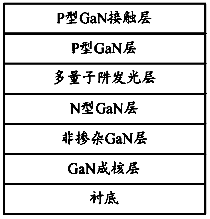
[0040] ginseng figure 1 Shown is a schematic diagram of the GaN-based LED epitaxial structure in the prior art, including from bottom to top: sapphire substrate, GaN nucleation layer, GaN buffer layer, non-doped GaN layer, N-type GaN layer, multi-quantum well light-emitting layer , a P-type GaN layer and a P-type GaN contact layer.

...


PUM


Abstract

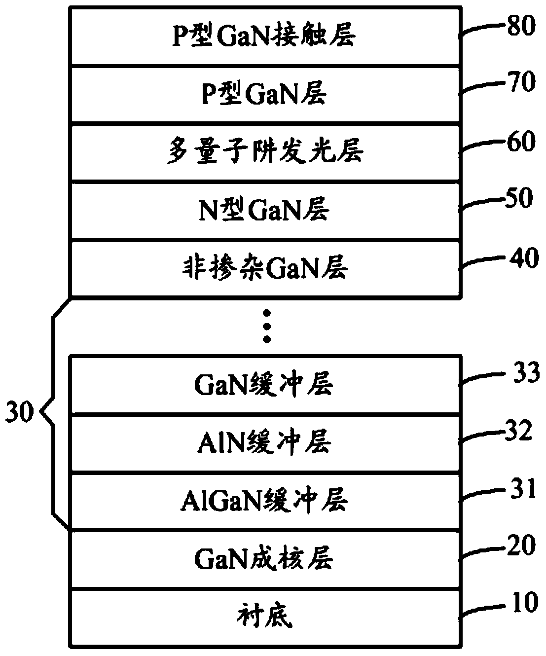
The invention discloses a GaN-based LED epitaxy structure and a preparation method thereof. The GaN-based LED epitaxy structure sequentially comprises a substrate, a GaN nucleating layer, a superlattice buffer layer, a non-doped GaN layer, an N type GaN layer, a multi-quantum-well luminescent layer, and a P type GaN layer, wherein the superlattice buffer layer adopts a superlattice structure which is prepared by alternately stacking a plurality of pairs of AlGaN buffer layers, AlN buffer layers and GaN buffer layers. The GaN-based LED epitaxy structure disclosed by the invention can relieve the lattice mismatch problem due to mismatch between the sapphire substrate and the GaN lattice, greatly reduces the warping of the epitaxial wafer during the whole high-temperature growth process, promotes the wavelength centrality and the yield of the epitaxial wafer, meanwhile effectively increases the GaN lattice quality, reduces the lattice dislocation density, and enables the optical-electrical characteristics of the device to be more stable.

Description

technical field [0001] The invention relates to the technical field of semiconductor light emitting devices, in particular to a GaN-based LED epitaxial structure and a preparation method thereof. Background technique [0002] A light-emitting diode (Light-Emitting Diode, LED) is a semiconductor electronic component capable of emitting light. This electronic component appeared as early as 1962. In the early days, it could only emit red light with low luminosity. Later, other monochromatic light versions were developed. Today, the light that can be emitted has covered visible light, infrared rays and ultraviolet rays, and the luminosity has also increased to a considerable extent. of luminosity. And the use is also used as indicator lights, display panels, etc. from the beginning; with the continuous advancement of technology, light-emitting diodes have been widely used in displays, TV lighting decoration and lighting. [0003] At present, commercial large-scale LED epitaxia...

Claims


Application Information

Patent Timeline
Patent Type & Authority Applications(China)
IPC IPC(8): H01L33/06H01L33/00
CPCH01L33/005H01L33/0075H01L33/02H01L33/06H01L33/12H01L33/20H01L2933/0008H01L2933/0066
Inventor 不公告发明人
Owner FOCUS LIGHTINGS SCI & TECH
Learn More