Wafer level packaging method for LED (Light-Emitting Diode) chip level white light source

A LED chip and wafer-level packaging technology, applied in semiconductor devices, electrical components, circuits, etc., can solve problems such as low yield, affecting LED yield, uneven color of LED product space, etc., to promote development and innovation, The effect of improving LED packaging efficiency and good overall color temperature consistency

Inactive Publication Date: 2015-03-04
WUHAN UNIV
View PDF2 Cites 24 Cited by
  • Summary
  • Abstract
  • Description
  • Claims
  • Application Information

AI Technical Summary

Problems solved by technology

Due to the high viscosity of the phosphor powder, the amount of phosphor powder varies greatly between different packaging modules during the process of coating the phosphor powder, resulting in a large change in the light color of the packaged LED product, which affects the consistency of the product. Because when the color temperature exceeds a certain range, LED products will not be able to be used, so it also affects the yield of LEDs and increases the cost of products
Moreover, in domestic packaging companies, phosphor glue is generally applied around the LED by dots to form a spherical cap-shaped phosphor shape. This shape will lead to uneven spatial colors of LED products, which will affect the lighting of LED product users. comfortability
To this end, it is necessary to develop a new LED phosphor coating process to overcome some shortcomings of the current packaging process, such as low color temperature consistency, low yield and low spatial color uniformity.

Method used


Image

  • Wafer level packaging method for LED (Light-Emitting Diode) chip level white light source
  • Wafer level packaging method for LED (Light-Emitting Diode) chip level white light source
  • Wafer level packaging method for LED (Light-Emitting Diode) chip level white light source

Examples


Embodiment 1

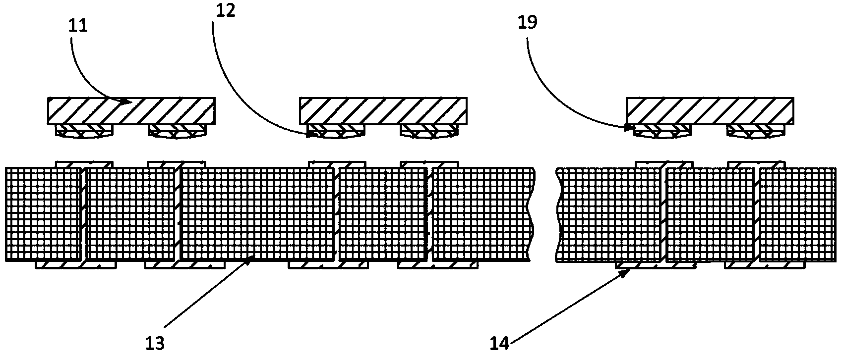
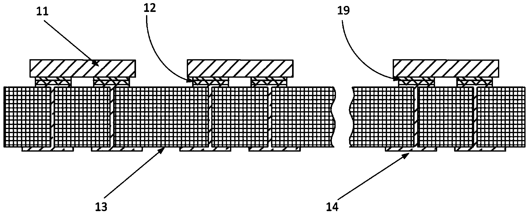
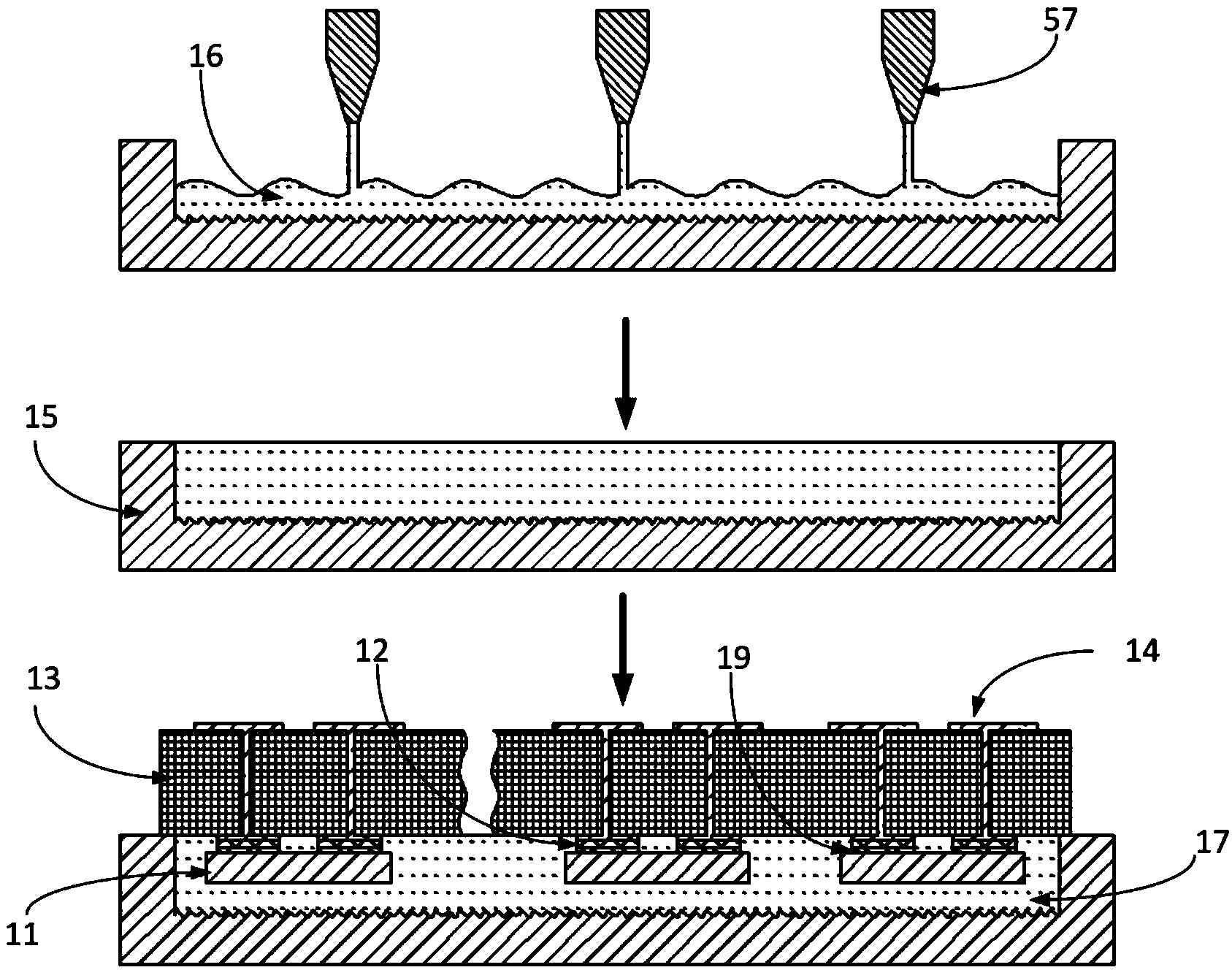
[0038] see Figure 1(a) and 1(b) , the LED flip chip 11 is integrated on the LED packaging wafer substrate 13 suitable for flip chip packaging through the solder layer 12 and the crystal bonding process, so as to realize the electrical connection and mechanical fixation of the flip chip electrode 19 and the substrate electrode 14 . Referring to Fig. 1(c), through the extrusion molding method with the surface roughening mold 15 containing the phosphor powder layer containing the phosphor powder glue 16, the LED wafer integrated with the LED flip chip is cured at a high temperature of 120°C to form a uniform Phosphor powder layer 17 with a thickness of 1.5 g / ml in the phosphor material used in the phosphor powder glue, and the thickness of the formed phosphor powder layer is 250 microns. Subsequently, the surface roughening mold 15 containing the phosphor layer is separated from the phosphor layer 17, and the encapsulation effect achieved is that a phosphor layer with a uniform...

Embodiment 2

[0040] see Figure 2(a) and 2(b), the LED flip chip 11 is integrated on the LED packaging wafer substrate 13 suitable for flip chip packaging through the solder layer 12 and the crystal bonding process, so as to realize the electrical connection and mechanical fixation of the flip chip electrode 19 and the substrate electrode 14 . Referring to Fig. 2 (c), through the extrusion molding method of the phosphor layer mold 21 containing the phosphor powder glue 16 and the phosphor layer with the phosphor layer prepared on the LED wafer integrated with the LED flip chip, through 120 The phosphor layer 22 with a convex structure is formed at a high temperature of ℃, and the concentration of the phosphor material in the phosphor glue used is 1.0 g / ml, and the thickness of the formed phosphor layer is 200 microns, and the height of the protrusion is 120 Microns. Subsequently, the surface roughening mold 15 containing the phosphor layer is separated from the phosphor layer 22 contain...

Embodiment 3

[0042] see Figure 3(a) and 3(b) , the LED flip chip 11 is integrated on the LED packaging wafer substrate 13 suitable for flip chip packaging through the solder layer 12 and the crystal bonding process, so as to realize the electrical connection and mechanical fixation of the flip chip electrode 19 and the substrate electrode 14 . Referring to FIG. 3( c ), the semi-cured phosphor layer film 31 used for wafer-level packaging is applied on the wafer by a vacuum embossing method to achieve a phosphor layer coating with a uniform thickness. Then the semi-cured phosphor layer film is cured at 120° C., wherein the concentration of the phosphor material in the phosphor layer film used is 2.0 g / ml, and the thickness of the formed phosphor layer is 150 microns. Then the support film 32 on the phosphor layer film 31 is peeled off by a robot. The encapsulation effect achieved is that a phosphor layer with a uniform thickness is coated on the wafer as shown in FIG. 3( d ). In order t...


PUM


Abstract

The invention discloses a wafer level packaging method for an LED chip level white light source. A packaging method of inverted LEDs comprises the following steps: firstly transferring the chips onto a wafer substrate plate (film), then carrying out fluorescent powder coating on a wafer sheet with a method that film vacuum press is obtained through a die, and finally carrying out cutting on the wafer sheet to obtain single LED direct white light source chips with chip levels. A packaging method of positive LEDs comprises the following steps: firstly completing solid crystal and gold thread bonding technology on a wafer substrate upper sheet for LED chips, then forming a silica gel protective lens with a spot-coating method for each LED chip, then coating uniform fluorescent powder layers on the silica gel protective lenses with a film vacuum pressing method, and finally carrying out cutting on the wafer sheet to obtain single LED direct white light source chips with chip levels. The LED packaging efficiency is greatly improved, an LED white light chip with good space color uniformity and overall color temperature consistency is obtained, and the development and innovation of LED packaging technology are greatly promoted.

Description

[0001] technical field [0002] The invention belongs to the technical field of LED packaging, and relates to a packaging method for realizing chip-level LED white light source packaging in LED packaging, and is particularly applied to realizing high-power LED wafer-level packaging. [0003] Background technique [0004] LED (Light Emitting Diode) is a semiconductor light-emitting device based on the principle of P-N junction electroluminescence. It has the advantages of high electro-optical conversion efficiency, long service life, environmental protection and energy saving, and small size. It is known as the green lighting source in the 21st century. If it can be applied to the field of traditional lighting, it will have a very significant energy-saving effect, which is of great significance in today's increasingly tense global energy sources. With the breakthrough of the third-generation semiconductor material technology represented by nitrides, the semiconductor lightin...

Claims


Application Information

Patent Timeline
Patent Type & Authority Applications(China)
IPC IPC(8): H01L33/50H01L33/48
CPCH01L33/502H01L33/005H01L33/48H01L2933/0041H01L2933/005
Inventor 刘胜郑怀陈斌郭醒雷翔占必红王国平周圣军
Owner WUHAN UNIV
Why Eureka
Try Eureka