Method for coating photoresist on surface of hydrophobic insulating layer

A hydrophobic insulating layer and surface coating technology, which is applied in the direction of electrical components, semiconductor/solid-state device manufacturing, circuits, etc., can solve the problems of adding modification and thermal reflow process, difficult to completely coat a large area, and high process cost , to achieve good photolithography process quality, ensure hydrophobic properties, and overcome difficult-to-control effects

Active Publication Date: 2015-03-11
SOUTH CHINA NORMAL UNIVERSITY +2
View PDF3 Cites 6 Cited by
  • Summary
  • Abstract
  • Description
  • Claims
  • Application Information

AI Technical Summary

Problems solved by technology

[0003] However, due to the low surface energy of the surface of the hydrophobic insulating material, it is difficult for the photoresist to directly adhere to its surface. At present, the main solution is: (1) Treat the surface of the hydrophobic material with plasma or ultraviolet ozone to make it hydrophilic However, this virtually increases the modification and thermal reflow process, and it is difficult to ensure that the surface hydrophobicity of the treated hydrophobic material can be completely restored, which not only increases the process complexity and cost, but also affects the electrowetting display device. work performance
(2) Another method is to form a layer of silicon dioxide or gold film as a sacrificial layer on the insulating layer by electron beam evaporation coating, then spin-coat the photoresist, and finally etch the sacrificial layer. Although this method can obtain Good effect, but requires high process cost and low efficiency, not suitable for large-area and industrialized production
[0004] Of course, there are also people who try to use high-viscosity photoresist to directly spin the photoresist on the hydrophobic surface, but because the current conventional photoresist coating process is to spin coat the photoresist through rapid heating methods such as hot air or light radiation, this The application range of this method is small, the success rate is relatively low, and it is difficult to ensure complete coating of a large area; further, it is difficult to control the thermal uniformity, and the coating will shrink to varying degrees during the spin coating process, and even after the coating is complete. It is prone to shrinkage or detachment of the coating, and the resulting coating has poor adhesion and uniformity

Method used


Image

  • Method for coating photoresist on surface of hydrophobic insulating layer
  • Method for coating photoresist on surface of hydrophobic insulating layer
  • Method for coating photoresist on surface of hydrophobic insulating layer

Examples


Embodiment Construction

[0025] The concept, specific structure and technical effects of the present invention will be clearly and completely described below in conjunction with the embodiments and accompanying drawings, so as to fully understand the purpose, features and effects of the present invention. Apparently, the described embodiments are only some of the embodiments of the present invention, rather than all of them. Based on the embodiments of the present invention, other embodiments obtained by those skilled in the art without creative efforts belong to The protection scope of the present invention. The various technical features in the invention can be combined interactively on the premise of not conflicting with each other.

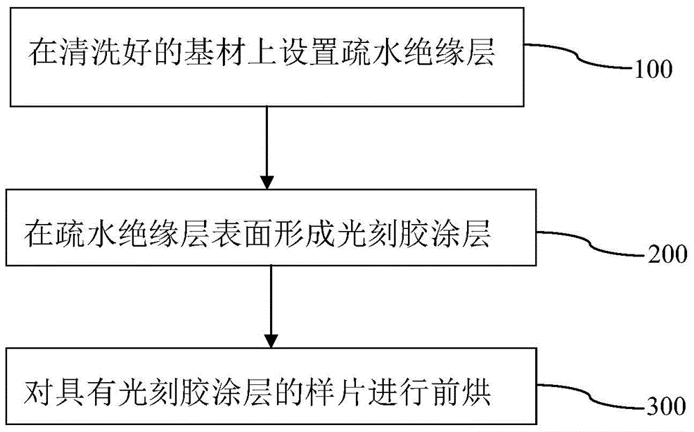
[0026] figure 1 It is a process flow chart of the photoresist coating method provided by the embodiment of the present invention.

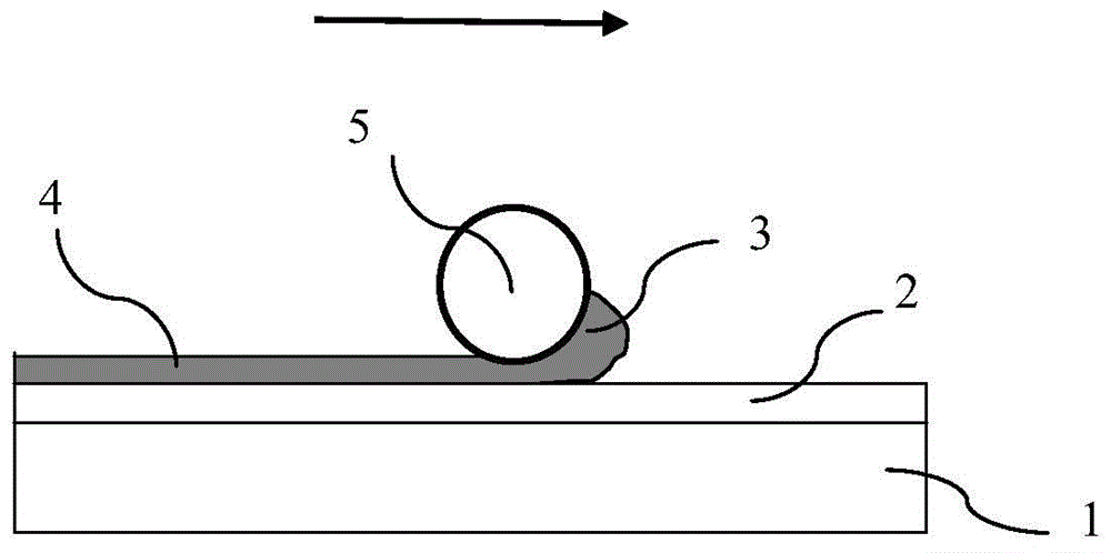
[0027] Step S100 , disposing a hydrophobic insulating layer 2 on the cleaned substrate 1 .

[0028] The substrate 1 is a substrate co...


PUM

PropertyMeasurementUnit
thicknessaaaaaaaaaa
thicknessaaaaaaaaaa

Abstract

The invention discloses a method for coating a photoresist on the surface of a hydrophobic insulating layer. The method comprises the steps of directly coating a photoresist solution with high viscosity on the surface of the hydrophobic insulating layer through a coil bar coating method; carrying out vacuum heating which is a special heat treatment method; strictly controlling temperature rise procedures, wherein the photoresist coating is good in viscosity, the bad viscosity phenomena of peeling, separating and the like cannot be caused on the coating in a developing process, and the good quality of a photolithography technique can be realized. The method provided by the invention can be used for electrowetting display, microflow control chip and other fields.

Description

technical field [0001] The invention relates to a method for coating photoresist on the surface of a hydrophobic insulating layer. Background technique [0002] Hydrophobic insulating materials are widely used in electrowetting display, microfluidic chip and other fields. As a new type of flat panel display technology, electrowetting display technology has the advantages of short response time, rich colors, wide viewing angle and low power consumption. In the display industry in the future, it has a very broad application market. A key preparation process of electrowetting display devices is to fabricate hydrophilic microarray display units on the surface of the hydrophobic insulating layer. Each display unit is a cofferdam formed by a photolithography process, and a pixel grid is formed by filling ink in the cofferdam and then encapsulating it. At present, the material surrounding the pixel grid is mainly photoresist material. [0003] However, due to the low surface ener...

Claims


Application Information

Patent Timeline
Patent Type & Authority Applications(China)
IPC IPC(8): H01L21/027
Inventor 水玲玲韦必明张茂榕金名亮周国富
Owner SOUTH CHINA NORMAL UNIVERSITY
Why Eureka
Try Eureka