Soi substrate bidirectional breakdown protection double gate insulation tunneling enhanced transistor and manufacturing method

A technology of breakdown protection and gate insulation, applied in SOI substrate bidirectional breakdown protection double-gate insulation tunneling enhanced transistor and its manufacturing field, can solve the problem of increasing tunneling probability transfer characteristics, increasing static power consumption, tunneling field Problems such as limited improvement of transfer characteristics of effect transistors

Inactive Publication Date: 2017-07-21
SHENYANG POLYTECHNIC UNIV
View PDF3 Cites 0 Cited by
  • Summary
  • Abstract
  • Description
  • Claims
  • Application Information

AI Technical Summary

Problems solved by technology

In addition, the continuous shortening of the channel length has led to an increase in the subthreshold swing of MOSFETs, which has resulted in severe degradation of switching characteristics and a significant increase in static power consumption.
Although the degradation of device performance can be alleviated by improving the gate electrode structure, when the device size is further reduced to below 20 nanometers, even with the optimized gate electrode structure, the subthreshold swing of the device will also decrease. increases with further reduction in device channel length, resulting in further deterioration of device performance;
[0005] Tunneling Field Effect Transistors (TFETs), compared with MOSFETs, although its average subthreshold swing has been improved, but its forward conduction current is too small. Narrow materials are used to generate the tunneling part of the tunneling field effect transistor, which can increase the tunneling probability to improve the transfer characteristics, but increases the difficulty of the process
In addition, the use of high dielectric constant insulating material as the insulating dielectric layer between the gate and the substrate can improve the control ability of the gate to the electric field distribution of the channel, but it cannot substantially increase the tunneling probability of the silicon material, so For the transfer characteristics of tunneling field effect transistors, the improvement is very limited

Method used


Image

  • Soi substrate bidirectional breakdown protection double gate insulation tunneling enhanced transistor and manufacturing method
  • Soi substrate bidirectional breakdown protection double gate insulation tunneling enhanced transistor and manufacturing method
  • Soi substrate bidirectional breakdown protection double gate insulation tunneling enhanced transistor and manufacturing method

Examples


Embodiment Construction

[0100] Below in conjunction with accompanying drawing, the present invention will be further described:

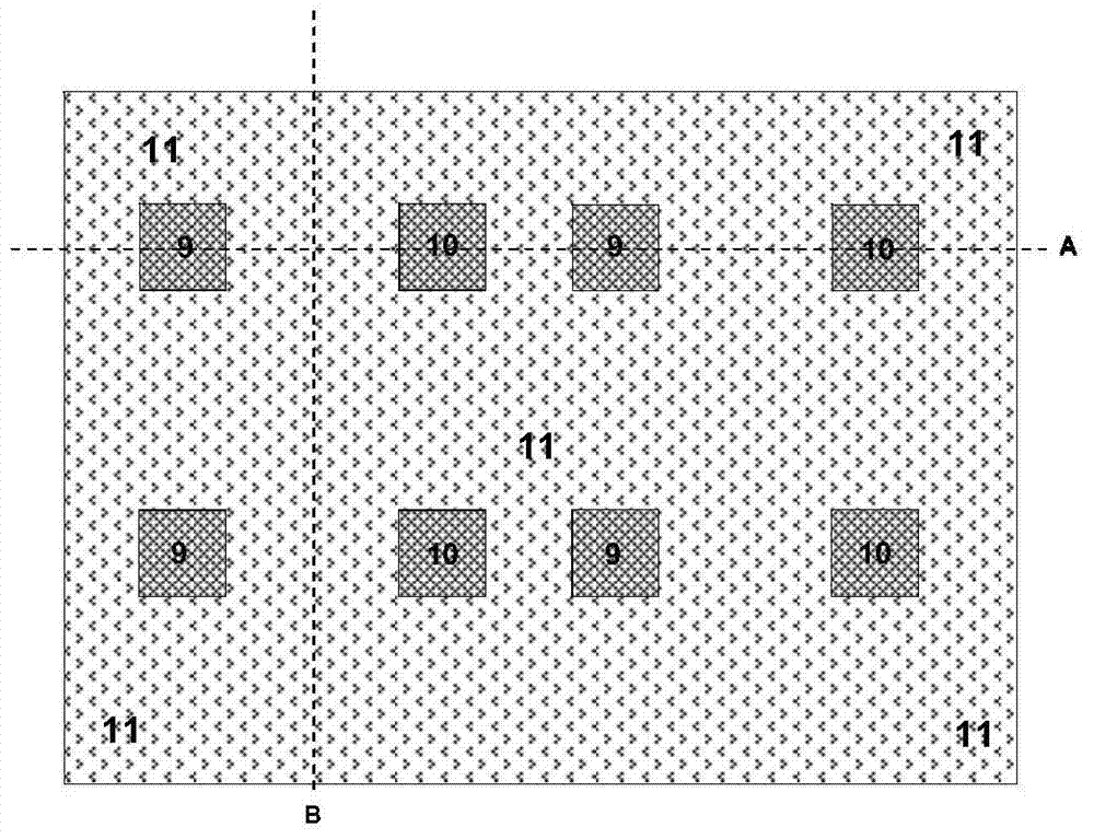
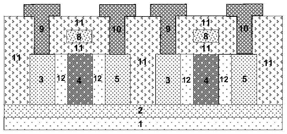
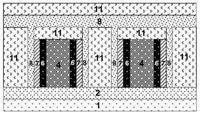
[0101] Such as figure 1 It is a top view schematic diagram of a two-dimensional structure of an SOI substrate bidirectional breakdown protection double-gate insulation tunneling enhancement transistor of the present invention; figure 2 yes figure 1 Schematic diagram of the cross-section obtained by cutting along the tangent line A; image 3 yes figure 1Schematic cross-sectional view obtained by cutting along tangent line B; specifically includes single crystal silicon substrate 1; wafer insulating layer 2; emitter region 3; base region 4; collector region 5; conductive layer 6; tunneling insulating layer 7; gate electrode 8 ; Emitter 9; Collector 10; Blocking insulating layer 11;

[0102] SOI substrate bidirectional breakdown protection dual-gate insulation tunneling enhanced transistor, using an SOI wafer including a single crystal silicon substrate 1 and a wafer ins...


PUM


Abstract

The invention relates to an SOI substrate bidirectional breakdown protection double-gate insulation tunneling enhancement transistor. Compared with MOSFETs or tunneling field effect transistors of the same size, the breakdown protection region with low impurity concentration is introduced into the collector junction and the emitter junction to prevent Significantly improve the forward and reverse withstand voltage capability of the device at the deep nanoscale; there are insulating tunneling structures on both sides of the base region, and the insulating tunneling effect occurs simultaneously in the base region under the control of the gate electrode On both sides, the generation rate of tunneling current is improved; excellent switching characteristics are achieved by utilizing the extremely sensitive relationship between the impedance of the tunneling insulating layer and its internal field strength; excellent forward conduction characteristics are achieved by enhancing the tunneling signal through the emitter ; In addition, the present invention also proposes a specific manufacturing method of SOI substrate bidirectional breakdown protection double-gate insulation tunneling enhancement transistor. The transistor significantly improves the working characteristics of the nanoscale integrated circuit unit and is suitable for popularization and application.

Description

[0001] Technical field: [0002] The invention relates to the field of ultra-large-scale integrated circuit manufacturing, and relates to an SOI substrate bidirectional breakdown protection double-gate insulation tunneling enhancement transistor and a manufacturing method thereof, which are suitable for manufacturing high-performance ultra-high integrated integrated circuits. [0003] Background technique: [0004] At present, with the continuous improvement of the integration level, the source electrode and the channel or between the drain electrode and the channel of the integrated circuit unit Metal Oxide Semiconductor Field Effect Transistor (MOSFETs) devices form a steep mutation PN within a few nanometers. Junction, when the drain-source voltage is large, this steep abrupt PN junction will have a breakdown effect, which will cause the device to fail. As the size of the device continues to shrink, this breakdown effect becomes more and more obvious. In addition, the contin...

Claims


Application Information

Patent Timeline
Patent Type & Authority Patents(China)
IPC IPC(8): H01L29/78H01L21/331
CPCH01L29/0684H01L29/6631H01L29/7311
Inventor 靳晓诗刘溪
Owner SHENYANG POLYTECHNIC UNIV
Why Eureka
Try Eureka