An InGaN-based blue-green light-emitting diode epitaxial structure and growth method

A technology of light-emitting diodes and epitaxial structures, applied to electrical components, circuits, semiconductor devices, etc., can solve problems such as mismatch and large lattice, and achieve the effect of reducing manufacturing costs

Active Publication Date: 2015-03-11
TAIYUAN UNIV OF TECH
View PDF8 Cites 19 Cited by
  • Summary
  • Abstract
  • Description
  • Claims
  • Application Information

AI Technical Summary

Problems solved by technology

[0005] The present invention provides an InGaN-based blue-green light-emitting diode in order to solve the problem of strong piezoelectric polarization field caused by the large lattice mismatch between InGaN and GaN in the active region in the existing GaN-based blue-green LED epitaxial structure. Epitaxial structure and growth method

Method used


Image

  • An InGaN-based blue-green light-emitting diode epitaxial structure and growth method
  • An InGaN-based blue-green light-emitting diode epitaxial structure and growth method

Examples


Embodiment 1

[0040] Embodiment 1 A method for growing an InGaN-based blue-green light emitting diode epitaxial structure includes the following steps:

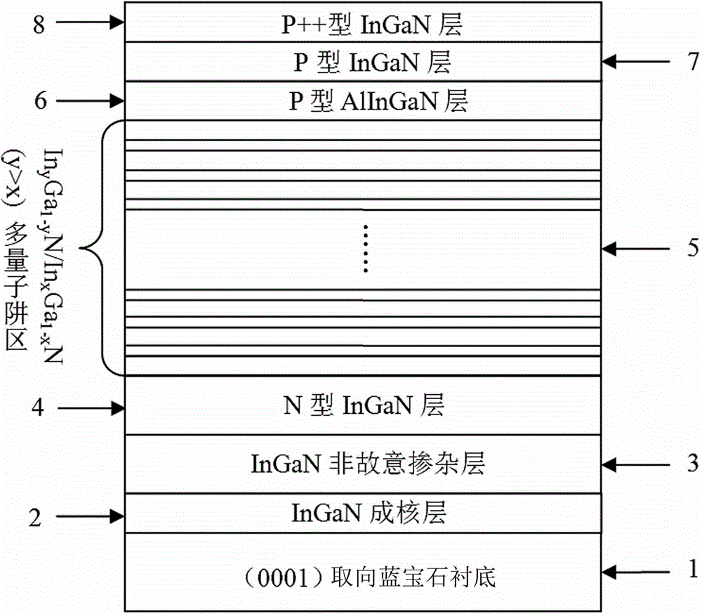
[0041] (1) Substrate annealing treatment: annealing the (0001) surface sapphire substrate in a hydrogen atmosphere at a temperature of 1060°C, then cooling to 580°C and introducing ammonia gas, and nitriding the substrate for 6 minutes;

[0042] (2) Growing a low-temperature InGaN nucleation layer: Change the hydrogen atmosphere to a nitrogen atmosphere, turn on the gallium source TMGa and indium source TMIn, and grow a 30nm thick InGaN nucleation layer at 580°C under the condition of 50sccm hydrogen gas. The pressure is 600mbar;

[0043] (3) Growing high-temperature InGaN unintentionally doped layer: turn off TMGa and TMIn, raise the temperature to 770°C, reduce the pressure to 150mbar, turn on TMGa and TMIn again, and grow a 1 micron unintentionally doped InGaN layer;

[0044] (4) Growing an n-type InGaN layer: keeping the growth temperature and...

Embodiment 2

[0050] Embodiment 2 A growth method of an InGaN-based blue-green light emitting diode epitaxial structure includes the following steps:

[0051] (1) Substrate annealing treatment: annealing the (0001) surface sapphire substrate in a hydrogen atmosphere at a temperature of 1060°C, then cooling to 580°C and introducing ammonia gas, and nitriding the substrate for 6 minutes;

[0052] (2) Growing a low-temperature InGaN nucleation layer: Change the hydrogen atmosphere to a nitrogen atmosphere, turn on the gallium source TMGa and indium source TMIn, and grow a 30nm thick low-temperature InGaN nucleation layer at 580°C under the condition of 50sccm hydrogen gas. The growth pressure is 600 mbar.

[0053] (3) Growing high-temperature InGaN unintentionally doped layer: turn off TMGa and TMIn, raise the temperature to 770°C, reduce the pressure to 150mbar, turn on TMGa and TMIn again, and grow a 1 micron unintentionally doped InGaN layer;

[0054] (4) Growing an n-type InGaN layer: keeping the ...


PUM

PropertyMeasurementUnit
thicknessaaaaaaaaaa
thicknessaaaaaaaaaa
thicknessaaaaaaaaaa

Abstract

The invention provides an InGaN-based blue-green light-emitting diode epitaxial growth method and a structure thereof, wherein the growth method of the epitaxial structure comprises specifically the following steps: performing a high temperature annealing process on a sapphire substrate in an ammonia atmosphere, reducing the temperature to 530-580 degrees and adjusting epitaxial growth atmosphere to grow a low temperature InGaN nucleation layer, and then raising the temperature and sequentially growing an InGan unintentionally doped layer, an n-type InGaN layer, an InyGa1-yN/InxGa1-xN(y> x) multi-quantum well active layer, A p-AlInGaN electron blocking layer, A p-type InGaN layer and the p++ type InGaN contact layer. The InGaN-based blue-green LED epitaxial structure provided in the present invention can effectively reduce the piezoelectric polarization field in an active area to thereby improve light emitting efficiency since the structure reduces lattice mismatch between a quantum well material and a matrix material.

Description

Technical field [0001] The invention relates to an InGaN-based blue-green light emitting diode epitaxial structure and growth method, belonging to the field of optoelectronic materials and devices. Background technique [0002] GaN-based high-brightness blue, green and white light-emitting diodes (LEDs) are widely used in many fields such as display and lighting due to their low energy consumption, long life, no pollution, and strong resistance to harsh environments. [0003] For traditional GaN-based blue-green LEDs, the basic structure of the active region is InGaN / GaN multiple quantum wells. Although GaN-based semiconductor materials and devices have achieved great development, there are still many scientific and technical problems to be solved. First, the question of the quantum confinement Stark effect in InGaN / GaN quantum wells. Since the lattice constant of InGaN is greater than that of GaN, in the InGaN / GaN quantum well grown along the [0001] direction, there is a gap bet...

Claims


Application Information

Patent Timeline
Patent Type & Authority Applications(China)
IPC IPC(8): H01L33/06H01L33/32H01L33/00
CPCH01L33/0075H01L33/0095H01L33/02H01L33/06H01L33/32H01L2933/0008H01L2933/0066
Inventor 翟光美李学敏梅伏洪张华马淑芳刘青明李小杜王皓田许并社
Owner TAIYUAN UNIV OF TECH
Why Eureka
Try Eureka