Resin composition for sealing semiconductor, semiconductor device with the cured product thereof and method for manufacturing semiconductor device

A resin composition and sealing technology, which can be used in semiconductor devices, semiconductor/solid-state device parts, electric solid-state devices, etc., can solve problems such as insufficient moisture resistance, reduced adhesion of CuLF, peeling or cracks, etc.

Active Publication Date: 2015-03-18
SHIN ETSU CHEM IND CO LTD
View PDF11 Cites 0 Cited by
  • Summary
  • Abstract
  • Description
  • Claims
  • Application Information

AI Technical Summary

Problems solved by technology

In addition, the composition described in Patent Document 2 has insufficient moisture resistance. Therefore, if it is left for a long period of time under high temperature and high humidity, the adhesion between CuLF or Ag plating and the cured product decreases, resulting in peeling or cracking.

Method used


Image

  • Resin composition for sealing semiconductor, semiconductor device with the cured product thereof and method for manufacturing semiconductor device
  • Resin composition for sealing semiconductor, semiconductor device with the cured product thereof and method for manufacturing semiconductor device
  • Resin composition for sealing semiconductor, semiconductor device with the cured product thereof and method for manufacturing semiconductor device

Examples


Embodiment

[0185] Hereinafter, examples and comparative examples are shown, and the present invention will be described in more detail, but the present invention is not limited to the following examples. In addition, the part in each example is a mass part.

[0186] [Example and Comparative Example]

[0187] Prepare the following components with the compositions shown in Table 1 to Table 6, mix them uniformly with a high-speed mixer, knead them uniformly with two heated rollers, cool them, and pulverize them to obtain a resin composition .

[0188] [Components (A) to (D) used in the first composition, the second composition, and the third composition]

[0189] (A) Cyanate compound

[0190] (a) Cyanate compound represented by the following formula (7) (Primaset (Primaset) PT-60, manufactured by Lonza Japan Co., Ltd., cyanoxy group equivalent: 119)

[0191] [chem 25]

[0192]

[0193] (mixture of n=0~10)

[0194] (b) Cyanate compound obtained in Synthesis Example 1 below

Synthetic example 1

[0196] 100 g of phenol compound MEH-7851SS (manufactured by Meiwa Kasei) was dissolved in 600 g of butyl acetate. The solution was cooled to about -15°C, and 32 g of gaseous cyanogen chloride was introduced. Next, 50 g of triethylamine was added dropwise with stirring over about 30 minutes while maintaining the temperature at -10°C or lower. After a further 30 minutes at the temperature, the cooling was stopped and the reaction mixture was filtered. The filtrate is then passed to an ion exchanger packed column. Next, the solvent was removed under reduced pressure at a bath temperature of 70°C, followed by removal of volatile impurities (including solvent residues, free triethylamine, di ethyl cyanamide). The obtained product was a cyanate compound represented by the following formula (8) (cyanooxy group equivalent weight: 208).

[0197] [chem 26]

[0198]

[0199] (mixture of n=0~10)

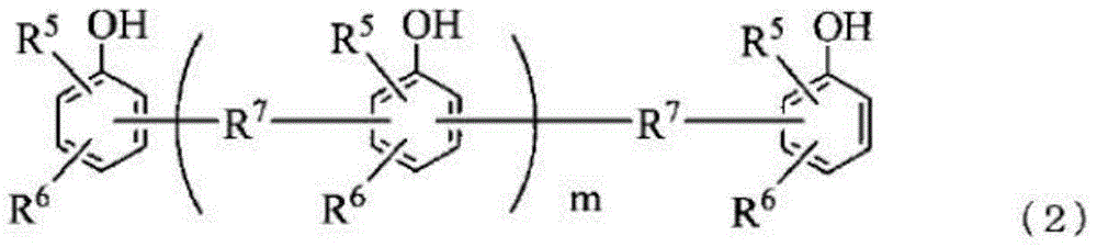
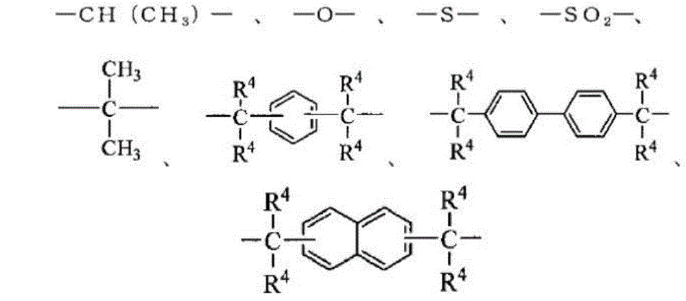
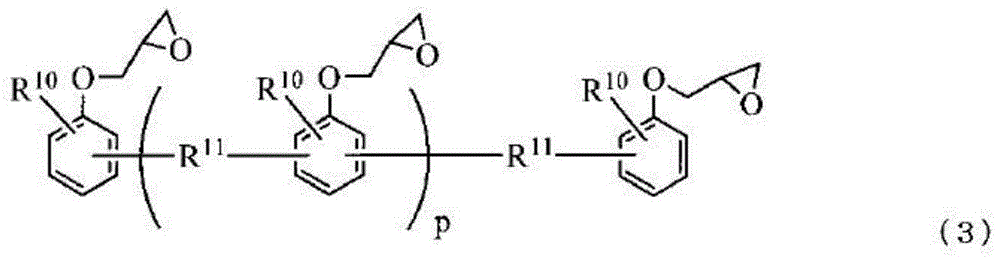
[0200] (B) Phenolic compounds

[0201] (c) A phenolic compound represented by the ...


PUM

PropertyMeasurementUnit
particle sizeaaaaaaaaaa

Abstract

The invention provides a resin composition for sealing a semiconductor, a semiconductor device with the cured product thereof and a method for manufacturing the semiconductor device. The resin composition for sealing a semiconductor contains (A) a cyanate ester compound with one molecule containing more than two cyanate oxygroups, (B) a phenol compound containing more than two phenol hydroxyls in one molecule, represented by the formula (2) and having a specific structure, (C) an inorganic filler, and (D) an epoxy resin having a specific structure and represented by the formula (3) or the formula (4), wherein the molar ratio of the phenol hydroxyls in the (B) phenol compound to the cyanate oxygroups in the (A) cyanate ester compound is 0.2-0.4, and the molar ratio of the epoxy groups in the (D) epoxy resin to the cyanate oxygroups in the (A) cyanate ester compound is 0.04-0.25.

Description

technical field [0001] The present invention relates to a resin composition for semiconductor sealing. Specifically, it relates to a composition that has excellent adhesion to copper (Cu) lead frame (LF) or silver (Ag) plating, and can form a composition that has excellent long-term thermal stability at high temperatures and can be used at high temperatures. A resin composition of a cured product that maintains adhesion to a metal substrate under high humidity and is excellent in reliability, and a semiconductor device having a cured product of the composition. [0002] In addition, the present invention relates to a resin composition for providing a semiconductor device with excellent long-term thermal stability under high temperature and high humidity, less corrosion or migration of Cu lead frame (LF), Ag plating, or Cu wire, and excellent reliability , and a semiconductor device having a cured product of the composition. [0003] Furthermore, the present invention relates...

Claims


Application Information

Patent Timeline
Patent Type & Authority Applications(China)
IPC IPC(8): C08L63/00C08K7/18C08K3/36C08K5/315C08G59/62C08K13/04C08K3/22C08K3/24C08K3/26C08K3/34H01L23/29
Inventor 长田将一萩原健司横田竜平
Owner SHIN ETSU CHEM IND CO LTD
Why Eureka
Try Eureka