

Organic electroluminescent device and preparation method thereof
An electroluminescent device and electroluminescent technology, which can be applied in the fields of electro-solid devices, semiconductor/solid-state device manufacturing, electrical components, etc., and can solve problems such as low light-emitting performance
- Summary
- Abstract
- Description
- Claims
- Application Information
AI Technical Summary
Problems solved by technology
Method used
Image

Examples
preparation example Construction
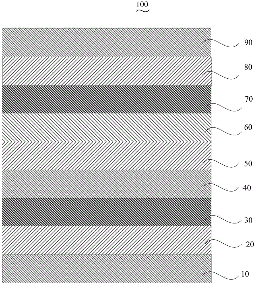
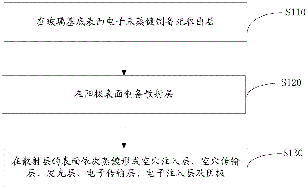
[0034] Please also see figure 2 , the preparation method of the organic electroluminescent device 100 of an embodiment, it comprises the following steps:
[0035] Step S110 , anode 20 on the surface of glass substrate 10 .
[0036] The glass substrate 10 is glass with a refractive index of 1.8-2.2, and the transmittance at 400 nm is higher than 90%. The glass substrate 10 is preferably glass with a grade of N-LAF36, N-LASF31A, N-LASF41A or N-LASF44.
[0037] The anode 20 is formed on one side surface of the glass substrate 10 . The material of the anode 20 is indium tin oxide (ITO), aluminum zinc oxide (AZO) or indium zinc oxide (IZO), preferably ITO. The thickness of the anode 20 is 80nm-300nm, preferably 120nm. The anode 20 is prepared by magnetron sputtering. The acceleration voltage of magnetron sputtering is 300-800V, the magnetic field is 50-200G, and the power density is 1-40W / cm 2 .
[0038] In this embodiment, the glass substrate 10 is rinsed with distilled wate...
Embodiment 1
[0053] The structure prepared in this example is glass / ITO / Li 2 CO 3 :Cu 2 O:NPB / WO 3 / NPB / BCzVBi / TAZ / CsF / Ag organic electroluminescence device.
[0054] The glass substrate is N-LASF44. After rinsing the glass substrate with distilled water and ethanol, soak it in isopropanol for one night. Magnetron sputtering anode on the glass substrate, the material is ITO, the thickness is 120nm; the scattering layer is prepared on the surface of the anode, and the material of the scattering layer includes Li 2 CO 3 、Cu 2 O and NPB, Li 2 CO 3 The mass ratio to CuI and NPB is 0.02:0.06:1, and the thickness is 250nm by electron beam evaporation. The energy density of electron beam evaporation is 40W / cm 2 . The hole injection layer was prepared by evaporation, and the material was WO 3 , the thickness is 30nm; the hole transport layer prepared by evaporation: the material is NPB, the thickness is 50nm; the light-emitting layer is prepared by evaporation: the selected material is ...
Embodiment 2
[0059] The structure prepared in this example is glass substrate / IZO / LiF:CuI:TAPC / MoO 3 / TAPC / ADN / Bphen / CsN 3 / Pt organic electroluminescent devices.
[0060] The high refractive index glass is N-LAF36. After the glass is rinsed with distilled water and ethanol, soak it in isopropanol for one night. An anode film was prepared on a high refractive index glass substrate, the material was IZO, and the thickness was 80nm. Then prepare the scattering layer, the material includes LiF, CuI and TAPC, the mass ratio of LiF to CuI and TAPC is 0.01:0.05:1, adopt electron beam evaporation, the thickness is 100nm, the energy density of electron beam evaporation is 100W / cm 2 . Evaporated hole injection layer: the material is MoO 3 , with a thickness of 40nm; evaporated hole transport layer: the material is TAPC, with a thickness of 45nm; evaporated luminescent layer: the selected material is ADN, with a thickness of 8nm; evaporated electron transport layer, the material is Bphen, with a...
PUM
| Property | Measurement | Unit |
|---|---|---|
| Thickness | aaaaa | aaaaa |
| Thickness | aaaaa | aaaaa |
| Power density | aaaaa | aaaaa |
Abstract
Description
Claims
Application Information