Avalanche photodiode and manufacturing method thereof

A technology of avalanche optoelectronics and manufacturing methods, which is applied in the direction of circuits, electrical components, semiconductor devices, etc., can solve the problems of large dark current, narrow superlattice band gap, and the inability to improve the signal-to-noise ratio, so as to reduce dark current, The effect of improving the signal-to-noise ratio

Active Publication Date: 2015-03-25
INST OF SEMICONDUCTORS - CHINESE ACAD OF SCI
View PDF2 Cites 21 Cited by
  • Summary
  • Abstract
  • Description
  • Claims
  • Application Information

AI Technical Summary

Problems solved by technology

However, the InAs / GaSb superlattice has a narrow band gap, and the dark current is large after being multiplied by an external high voltage, so it is impossible to improve the signal-to-noise ratio

Method used


Image

  • Avalanche photodiode and manufacturing method thereof

Examples


Embodiment Construction

[0013] In order to make the object, technical solution and advantages of the present invention clearer, the present invention will be further described in detail below in conjunction with specific embodiments and with reference to the accompanying drawings.

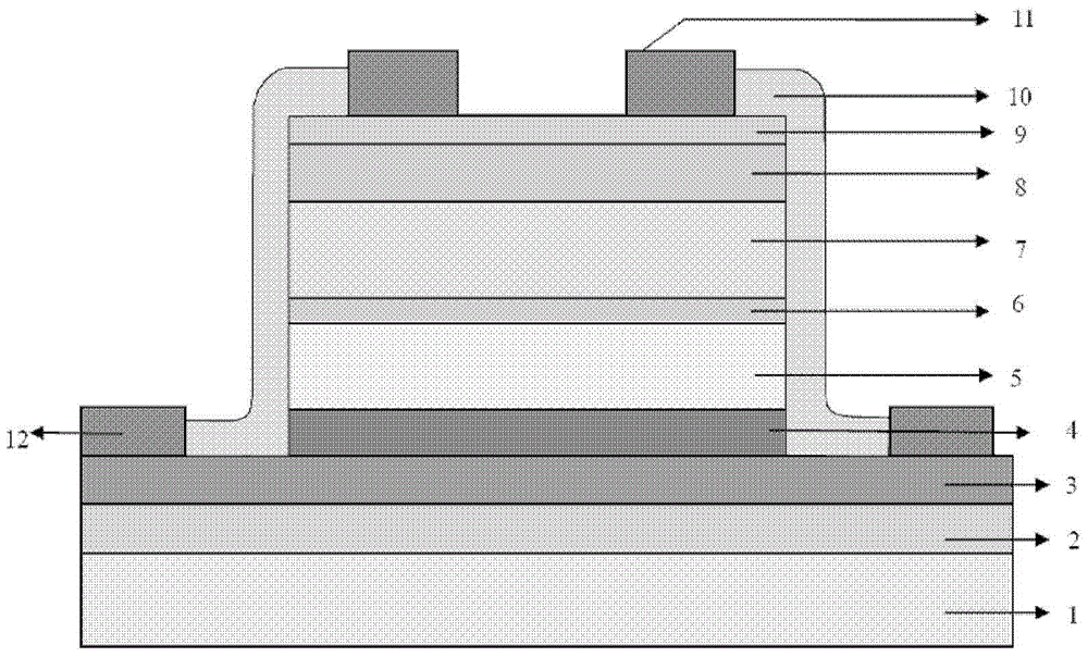
[0014] figure 1 is a schematic cross-sectional view of an avalanche diode in an embodiment of the present invention. Such as figure 1 shown, the avalanche diode consists of:

[0015] GaSb substrate 1;

[0016] GaSb buffer layer 2, which is epitaxially grown on the substrate 1;

[0017] N-type ohmic contact layer 3 grown on the buffer layer 2;

[0018] The mesa, which is located on the N-type ohmic contact layer 3, includes:

[0019] N-region charge layer 4, which grows on N-type ohmic contact layer 3;

[0020] Avalanche multiplication layer 5, which grows on the upper surface of charge layer 4 in N region;

[0021] A charge stop layer 6 grown on the upper surface of the avalanche multiplication layer 5;

[0022] A...


PUM


Abstract

The invention discloses an avalanche photodiode and a manufacturing method of the avalanche photodiode. The avalanche photodiode comprises a buffering layer at least having epitaxial growth on a substrate, an N-type ohmic contact layer, a light absorption layer, an avalanche multiplication and a P-type ohmic contact layer. The light absorption layer is made of superlattices of an InAs layer and a GaSb layer which are different in thickness and can adsorb infrared from a short wave to a long wave, meanwhile, dark current can be reduced by AlGaAsSb, the device is manufactured through mesa etching, passivation and metal evaporation, the device can respond to the infrared from the short wave to the long wave and provide certain gain, and therefore the signal-to-noise ratio of a detector can be increased.

Description

technical field [0001] The invention relates to the technical field of semiconductors, in particular to an avalanche photodiode for mid-wave infrared. Background technique [0002] Avalanche photodiodes (APDs) are widely used in civil and military fields such as optical fiber optical transmission systems, strategic early warning, guidance sensing, and lidar, because avalanche photodiodes significantly improve the sensitivity of light detection and faster response speed. However, the cut-off wavelength of lattice-matched InGaAs avalanche photodiodes based on InP substrates does not exceed 1.7 microns, while the material quality of avalanche photodiodes with mismatched lattices epitaxially is not good enough to achieve high performance. However, the mercury cadmium telluride infrared detector that can be extended to the mid-wave infrared band has a difficult substrate, a low yield, and poor material growth uniformity, resulting in high cost of the manufactured avalanche diode....

Claims


Application Information

Patent Timeline
Patent Type & Authority Applications(China)
IPC IPC(8): H01L31/107H01L31/0352H01L31/0304H01L31/18
CPCH01L31/0304H01L31/03046H01L31/035236H01L31/107H01L31/18
Inventor 向伟王国伟徐应强郝宏玥蒋洞微任正伟贺振宏牛智川
Owner INST OF SEMICONDUCTORS - CHINESE ACAD OF SCI
Why Eureka
Try Eureka