Method for improving metal silicides
A metal silicide, metal layer technology, applied in electrical components, semiconductor/solid-state device manufacturing, semiconductor devices, etc., can solve the problems that have not been introduced, and achieve the effect of increasing the fluorine content
- Summary
- Abstract
- Description
- Claims
- Application Information
AI Technical Summary
Problems solved by technology
Method used
Image
Examples
specific Embodiment 1
[0027] The present invention relates to a kind of method for improving existing nickel silicide, which comprises the following steps:
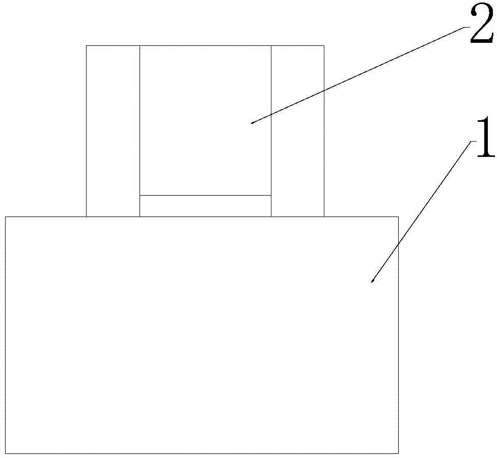
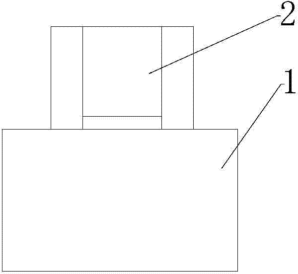
[0028] Such as figure 1 As shown in step S1, a gate structure is formed on a silicon substrate 1 pre-prepared with a metal silicide preparation region, and the gate structure includes a gate oxide layer 2 and a gate located above the gate oxide layer 2. The electrode 3 and the gate 3 can be metal gates or polysilicon gates, which are selected according to the needs of actual devices;
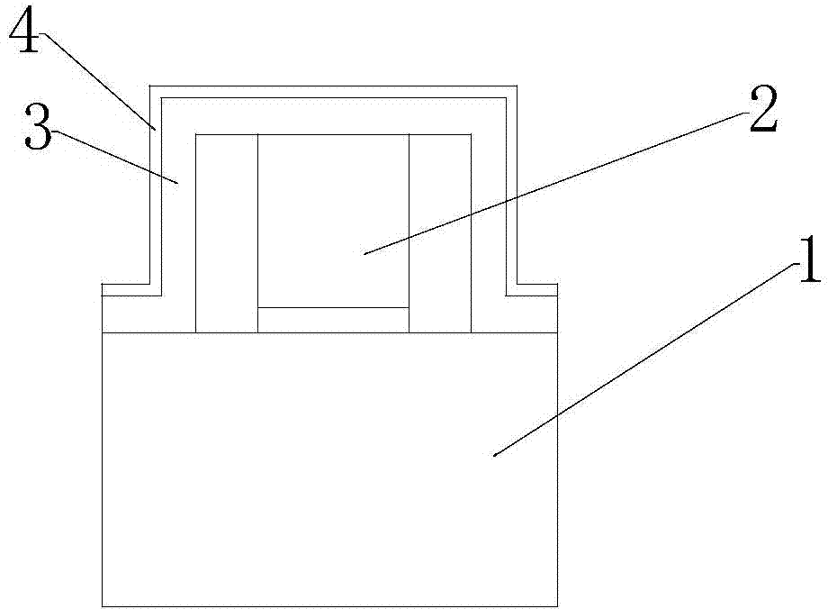
[0029] Such as figure 2 As shown, in step S2, a layer of fluorine-doped silicon oxide layer 4 is deposited on the surface of the remaining silicon substrate 1, the upper surface of the gate 3 and the side surfaces of the gate structure. The thickness of the fluorine-doped silicon oxide layer 4 is preferably 20 -100 Angstroms, wherein the content of fluorine is preferably less than 5%, and then depositing a silicon nitride layer 5 on the surface of the fluori...
specific Embodiment 2
[0034] Such as Figure 1 to Figure 5 Shown, the present invention relates to a kind of method for improving existing nickel silicide, which comprises the following steps:
[0035] Such as figure 1 As shown in step S1, a gate structure is formed on a silicon substrate 1 pre-prepared with a metal silicide preparation region, and the gate structure includes a gate oxide layer 2 and a gate located above the gate oxide layer 2. The electrode 3 and the gate 3 can be metal gates or polysilicon gates, which are selected according to the needs of actual devices;
[0036] Step S2, depositing a silicon oxide layer (not shown in the figure) on the surface of the remaining silicon substrate 1, the upper surface of the gate 3 and the sides of the gate structure;
[0037] Such as figure 2 As shown, in step S3, a layer of fluorine-doped silicon oxide layer 4 is deposited on the upper surface of silicon oxide to form a silicon oxide composite layer. The thickness of the fluorine-doped sil...
specific Embodiment 3
[0042] The present invention relates to a kind of method for improving existing nickel silicide, which comprises the following steps:
[0043]Step S1, forming a plurality of gate structures on a silicon substrate pre-prepared with a metal silicide preparation region, these gate structures include a gate oxide layer and gates located above these gate oxide layers, the gates can be The metal gate can also be a polysilicon gate, which is selected according to the needs of the actual device;
[0044] Step S2, depositing a layer of fluorine-doped silicon oxide layer on the surface of the remaining silicon substrate, the upper surface of the gate and the side of the gate structure, the thickness of the fluorine-doped silicon oxide layer is preferably 20-100 angstroms, wherein the fluorine The content is preferably less than 5%, and then a silicon nitride layer is deposited on the surface of the fluorine-doped silicon oxide layer;
[0045] Step S3, performing a first heat treatment ...
PUM
| Property | Measurement | Unit |
|---|---|---|
| Thickness | aaaaa | aaaaa |
Abstract
Description
Claims
Application Information
 - R&D Engineer
- R&D Manager
- IP Professional
- Industry Leading Data Capabilities
- Powerful AI technology
- Patent DNA Extraction
Browse by: Latest US Patents, China's latest patents, Technical Efficacy Thesaurus, Application Domain, Technology Topic, Popular Technical Reports.
© 2024 PatSnap. All rights reserved.Legal|Privacy policy|Modern Slavery Act Transparency Statement|Sitemap|About US| Contact US: help@patsnap.com


