Technique for Etching Monolayer and Multilayer Materials

a technology of monolayer and multilayer materials, applied in the direction of nanoinformatics, basic electric elements, nuclear engineering, etc., can solve the problems of less desirable multi-step processes, less etching, and less etching, so as to reduce the consumption of nickel hard-masks, the effect of high vertical anisotropy and adequate surface roughness

Active Publication Date: 2012-08-16
UCHICAGO ARGONNE LLC +1
View PDF18 Cites 13 Cited by
  • Summary
  • Abstract
  • Description
  • Claims
  • Application Information

AI Technical Summary

Benefits of technology

[0012]Also, in accordance with the first embodiment, the RIE technique can be used in combination with ICP and the fluorine-based chemistry component containing a gas mixture of SF6 and O2. The disclosed process has been found to provide higher etching rates of monolayer and multilayer materials of silicide-based metals with SF6, as compared to traditional CF4, and vertical anisotropy is increased by high fluorine content within the plasma. According to this embodiment, highly anisotropic etching of up to about a 9.0 micron-thick WSi2 / Si multilayer can be achieved by using a combined RIE / ICP process with a SF6 and O2 gas mixture (fluorine chemistry alone). Additionally, according to this embodiment, vertical etching can be sustained by the physical etching via ion bombardment for high fluorine content plasmas, while lateral etching is limited by the oxygen reaction with the materials. Furthermore, the sidewalls of the etched structures have adequate surface roughness for use as transmission optics used for example in x-ray focusing when etched with either the CF4 / O2 or SF6 / O2 chemistry.
[0016]In accordance with the second embodiment, the present disclosure provides for sectioning by etching of monolayer and multilayer materials using the combined RIE / ICP process with a combination of fluorine-based and chlorine-based chemistries. According to this embodiment, a high level of vertical anisotropy is achieved by a gas mixture of fluorine- and chlorine-based chemistries; namely, CHF3, Cl2, and O2 with radio frequency (RF) power and inductively coupled plasma (ICP) power. According to this embodiment, deeper etching (e.g., over 5 microns, preferably over 8 microns, and more preferably over 20 microns) and straighter sidewalls can be achieved with the disclosed process as compared to traditional etching using SF6 and CF4.
[0019]Additionally, a passivation layer can be formed on the surface of the monolayer or multilayer material which aids in anisotropic profile generation. Consumption of a masking material such as a nickel hard-mask can be reduced with this second embodiment. producing a series of etched tungsten silicide / silicone multilayers comprising sidewalls having a high degree of vertical anisotropy, a surface with adequate surface roughness for transmission optics, and a passivation layer on the surface after being etched. The etching is performed using RF power and ICP power.

Problems solved by technology

Due to the intrinsic differing chemistries related to reactivity, ion bombardment, and passivation of materials, the development of recipes for new materials or material systems can require intense effort and resources.
Multi-step processes are less desirable as the sidewall profile is “scalloped” in most cases.
When this stack is sectioned to allow side-illumination with radiation, the diffracted exiting radiation will constructively interfere at the focal point.
The traditional technique for sectioning multilayer Laue lens (MLL) involves mechanical sectioning and polishing, which is labor intensive and can induce delamination or structure damage and thereby reduce yield (Kang, H. C., Stephenson, G. B., Liu, C., Conley, R., Khachatryan, R., Wieczorek, M., Macrander, A. T., Yan, H., Maser, J., Hiller, J., Koritala, R., “Sectioning of multilayers to make a multilayer Laue lens”, Rev. Sci. Instr. 78, 046103-1-3 (2007)).
However, well-performing reactive ion etching recipes have been developed for only a small number of materials, and even less recipes exist for concurrent etching of more than one element so a fully material specific process needs to be developed.
Further, the techniques are limited with respect to the shapes of the device to be produced,
Additionally, according to this embodiment, vertical etching can be sustained by the physical etching via ion bombardment for high fluorine content plasmas, while lateral etching is limited by the oxygen reaction with the materials.

Method used


Image

  • Technique for Etching Monolayer and Multilayer Materials
  • Technique for Etching Monolayer and Multilayer Materials
  • Technique for Etching Monolayer and Multilayer Materials

Examples


examples

1. Multilayer Substrate Preparation

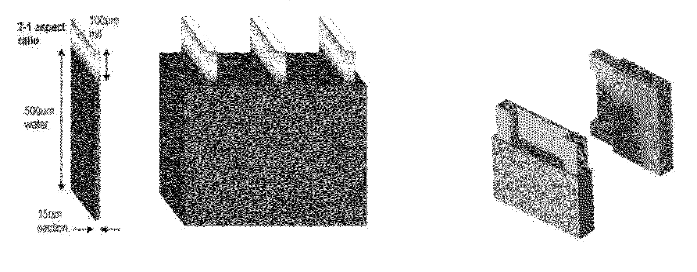
[0116]The multilayers are prepared by DC magnetron sputtering under high vacuum onto Si (100) wafers. Layers are deposited by raster-scanning the substrate over stationary targets with figured apertures at well-defined velocities using a rotary deposition system in the BNL, NSLS-II deposition laboratory using a method that has been previously reported (Conley, R., Liu, C., Kewish, C. M., Macrander, A. T., Morawe, C., “Multilayer growth in the APS rotary deposition system”, Proc. SPIE 6705, 670505 (2007); Conley, R., et al., “Wedged multilayer Laue lens”, Rev. Sci. Instr. 79, 053104 (2008); and Kang, H., et al., “Nanometer Linear focusing of Hard X Rays by a Multilayer Laue Lens”, Phys. Rev. Letters 96, 127401 (2006); each of which is herein incorporated by reference). Sputtering targets with dimensions of 3 inch diameter and 0.25″ thick are comprised of boron-doped silicon and hot-pressed WSi2. Initial tests utilize very simple periodic multilayer ...

example 2

CF4 / O2 Etching (Prior Art)

[0121]Initial tests were performed using a CF4 / O2 gas mixture due to reports in the literature which indicate, separately, that this particular gas combination has successfully etched both Si and WSi2 (Oehrlein, G. S., Lindstom, L. J., “Competitive reactions of fluorine and oxygen with W, WSi2, and Si surfaces in reactive ion etching using CF4 / O2”, Journal of Vacuum Science &Technology A: Vacuum, Surfaces, and Films 7 (3), 1035-1041 (1989); Abe, H., Yoneda, M., Fujiwara, N., “Developments of Plasma Etching Technology for Fabricating Semiconductor Devices”, Jap. J. of Appl. Phys. 47 (3), 1435-1455 (2008); and Lee, Y. H., Chen, M.-M., Ahn, K. Y., Bright, A. A., “Reactive etching mechanism of tungsten silicide in CF4-O2 plasma”, Thin Solid Films 118 (2), 149-154 (1984); all of which are herein incorporated by reference). CF4 provides fluorine radicals to perform the chemical etching of both Si and WSi2, and oxygen acts as a passivation agent on the sidewalls, ...

example 3

SF6 / O2 etching

[0124]A. First Embodiment with RIE Only and Fluorine Chemistry Only

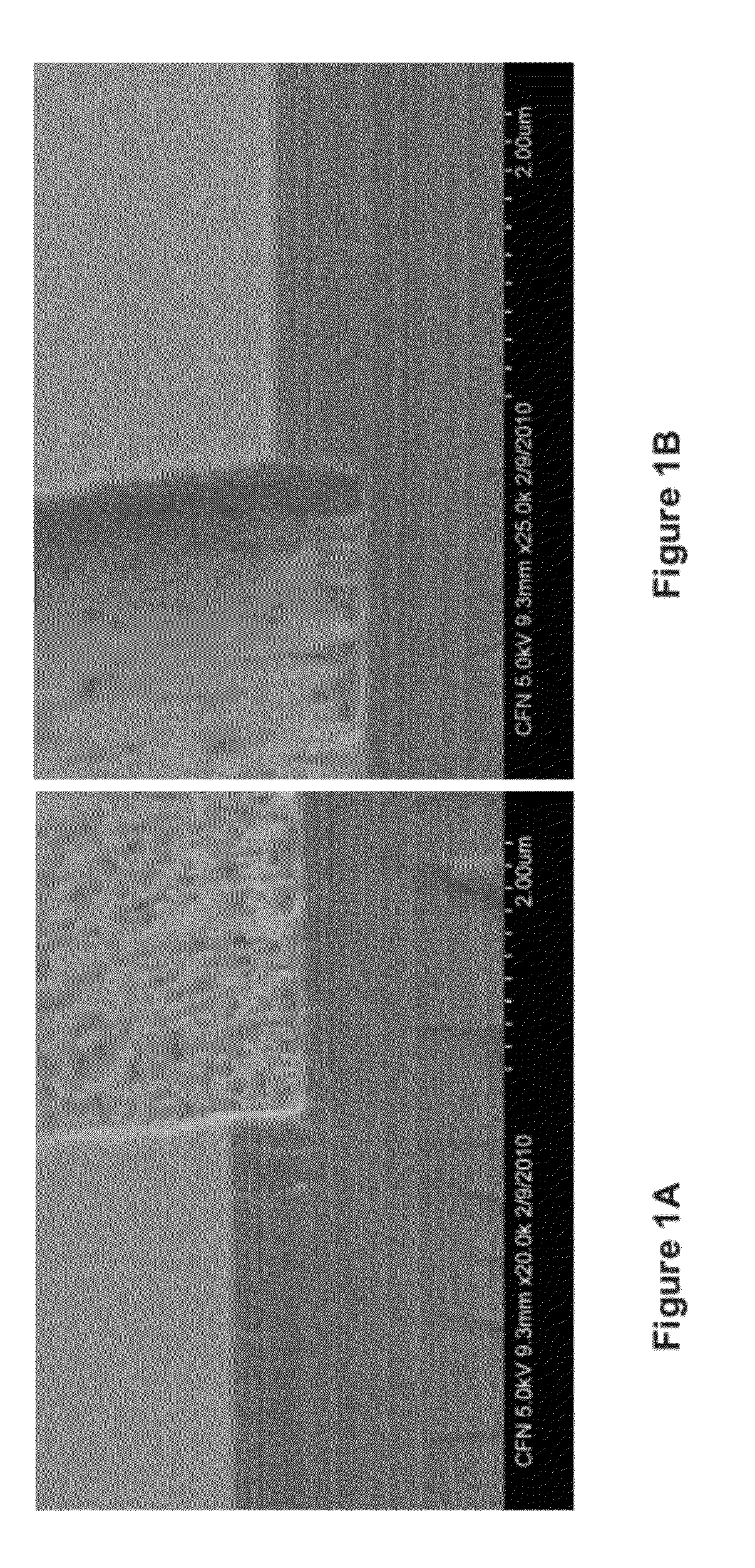
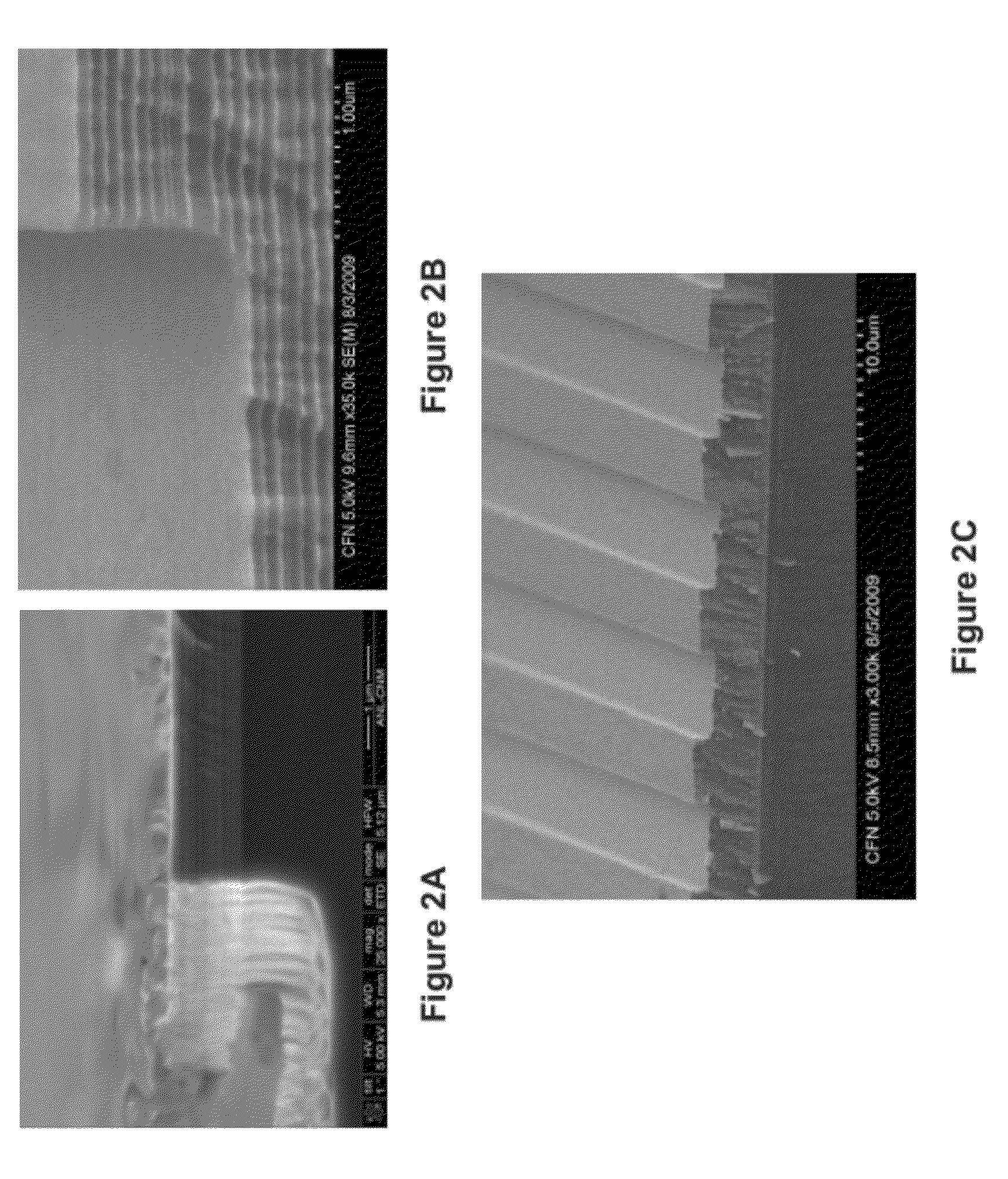
[0125]One advantage that SF6 brings over CF4 is that more fluorine radicals are available to react with the multilayer materials. When etching Si only, SF6 has been shown in other studies to realize a faster etching rate when compared to CF4 (Buyanova, I. A., Henrya, A., Monemara, B., Lindströmb, J. L., Oehrlein, G. S., “Photoluminescence characterization of SF6—O2 plasma etching of silicon”, Materials Science and Engineering B36, 100-103 (1996); which is herein incorporated by reference). The initial experimental conditions used for this gas, SF6, are chosen to be very similar to those employed for the CF4 / O2 chemistry. FIG. 2 illustrates typical cross-section profiles of a multilayer of WSi2 / Si etched by RIE using a mixture of 91% SF6 / 9% O2 at a pressure of 25 mTorr using an RF power of 250 W at room temperature at the CFN at BNL (FIG. 2C) and at −30° C. (FIG. 2B); RF power of 100 W at room temperatur...


PUM

PropertyMeasurementUnit
radio frequency poweraaaaaaaaaa
inductively coupled plasma poweraaaaaaaaaa
pressureaaaaaaaaaa

Abstract

A process is disclosed for sectioning by etching of monolayers and multilayers using an RIE technique with fluorine-based chemistry. In one embodiment, the process uses Reactive Ion Etching (RIE) alone or in combination with Inductively Coupled Plasma (ICP) using fluorine-based chemistry alone and using sufficient power to provide high ion energy to increase the etching rate and to obtain deeper anisotropic etching. In a second embodiment, a process is provided for sectioning of WSi2 / Si multilayers using RIE in combination with ICP using a combination of fluorine-based and chlorine-based chemistries and using RF power and ICP power. According to the second embodiment, a high level of vertical anisotropy is achieved by a ratio of three gases; namely, CHF3, Cl2, and O2 with RF and ICP. Additionally, in conjunction with the second embodiment, a passivation layer can be formed on the surface of the multilayer which aids in anisotropic profile generation.

Description

[0001]This application claims the benefit of U.S. Provisional Application No. 61 / 442,040, filed Feb. 11, 2011, entitled “Technique for Etching WSi2 and Si based Materials” and U.S. Provisional Application No. 61 / 504,013, filed Jul. 1, 2011, entitled “Technique for Etching Monolayer and Multilayer Materials”, both of which are hereby incorporated by reference in their entirety.STATEMENT OF GOVERNMENT LICENSE RIGHTS[0002]The present invention was made with Government support under contract numbers DE-AC-02-98CH10886 and DE-AC02-06CH11357, awarded by the U.S. Department of Energy. The Government has certain rights in the invention.I. FIELD OF THE INVENTION[0003]This invention relates generally to reactive ion etching for monolayer and multilayer materials. In particular, the present invention relates to a deep etching of monolayer and multilayer materials, such as a WSi2 / Si Multilayer Laue Lens (MLL), using reactive ion etching with a combination of fluorine-based and chlorine chemistr...

Claims


Application Information

Patent Timeline
Patent Type & Authority Applications(United States)
IPC IPC(8): H01L23/58H01L21/3065
CPCH01L21/3065G21K1/062B82Y10/00G21K2201/067C23F4/00H01L21/32137
Inventor BOUET, NATHALIE C.D.CONLEY, RAYMOND P.DIVAN, RALUMACRANDER, ALBERT
Owner UCHICAGO ARGONNE LLC
Why Eureka
Try Eureka