Device and method for monitoring dislocation of loaded wafer of flat plate type epitaxial furnace

A monitoring device and epitaxial furnace technology, which are applied in the fields of semiconductor/solid-state device testing/measurement, electrical components, semiconductor/solid-state device manufacturing, etc. Timely discovery of electrical parameter problems and other problems to avoid serious losses to manufacturers

Inactive Publication Date: 2015-04-08
HANGZHOU LION MICROELECTRONICS CO LTD
View PDF6 Cites 32 Cited by
  • Summary
  • Abstract
  • Description
  • Claims
  • Application Information

AI Technical Summary

Problems solved by technology

As we all know, for semiconductor devices, the epitaxial layer needs to have a perfect crystal structure and uniform electrical parameters such as epitaxial thickness and resistivity. The appearance of out of pocket makes the temperature and air flow on the silicon wafer change during the epitaxy process, which directly leads to the deterioration of the epitaxial wafer thickness and resistivity uniformity, and even produces lattice defects.
[0004] The current popular flat-panel epitaxy equipment cannot detect the out of pocket of the silicon wafer, and after the manipulator completes the loading of the silicon wafer, it is impossible to manually identify the abnormality
Once out of pocket occurs, the epitaxial wafer parameters will be out of control
In the actual production of epitaxial wafers, since the test method of the main parameters such as the resistivity test is a destructive test, the sampling test of producing 25 t...

Method used


Image

  • Device and method for monitoring dislocation of loaded wafer of flat plate type epitaxial furnace
  • Device and method for monitoring dislocation of loaded wafer of flat plate type epitaxial furnace
  • Device and method for monitoring dislocation of loaded wafer of flat plate type epitaxial furnace

Examples


Embodiment 1

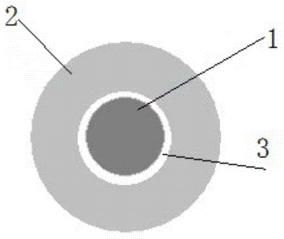
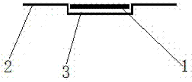
[0032] This embodiment applies the chip dislocation (out of pocket) monitoring device of the present invention in the ASM monolithic epitaxy furnace commonly used in the industry at present, and a reaction chamber of the ASM monolithic epitaxy furnace has only one carrier slot, and the present embodiment is used The loading sheet is a single-sided polished silicon wafer. Such as Figure 3aAs shown: a laser transmitter 5 is installed on one side of the outside of the quartz cover 4 in the reaction chamber of the epitaxial furnace, and a laser receiver 6 is installed on the other side outside the quartz cover, which is used for laser detection in out of pocket monitoring Transmitting and receiving; the laser transmitter 5 and the laser receiver 6 are respectively connected to the laser detection & control substrate 7, and the laser detection & control substrate 7 is used as the signal transmission, reception and processing between the laser transmitter 5 and the laser receiver 6...

Embodiment 2

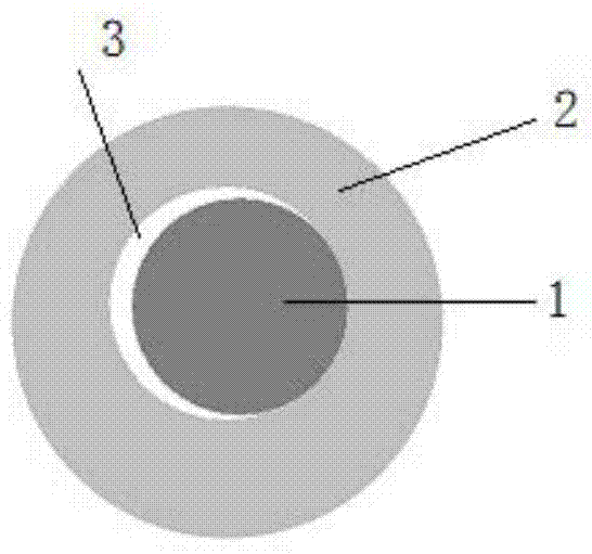
[0042] In this embodiment, the out of pocket monitoring device of the present invention is applied to the LPE3061 epitaxial furnace widely used in the current flat-plate epitaxial furnace. A generation of discrete device technology, IGBT, PowerMos and thin layers, buried layers, and because it is heated by a low-frequency power generator, it can save electricity. The quality of epitaxial wafers is close to that of single-chip furnace products, and the cost is close to that of high-capacity epitaxial furnaces. It is the only epitaxial reaction furnace that can deposit epitaxial films with a thickness of more than 200 microns, so it is currently a common equipment for silicon epitaxial wafer manufacturers. The base of LPE3061 has multiple loading slots 3, which can produce multiple epitaxial wafers at the same time. When loading the wafers, the manipulator 8 automatically loads the loaded wafers in such Figure 5 As shown in the slide slot 3 of the slide loading position corresp...


PUM


Abstract

The invention provides a device and a method for monitoring the dislocation of a loaded wafer of a flat plate type epitaxial furnace. The device comprises a loaded wafer, a base of the epitaxial furnace, a loaded wafer groove, a mechanical hand, a laser transmitter, a laser receiver, a laser detection and control substrate and the like, wherein the laser detection and control substrate is mutually connected with a mechanical hand detection and control substrate of the epitaxial furnace and a machine table main control system. After the loading of the loaded wafer is completed, laser light is emitted to a center position of the loaded wafer of the epitaxial furnace substrate through the laser transmitter, and the laser light is reflected through the loaded wafer; the laser receiver is used for receiving the reflected laser light, and the monitoring of dislocation of the loaded wafer is carried out by judging whether the laser light is received by the laser receiver or not. According to the device and the method for monitoring the dislocation of the loaded wafer of the flat plate type epitaxial furnace, provided by the invention, the situation that a loaded wafer is subjected to dislocation can be accurately and effectively detected at the first time after the loading of the loaded wafer is completed, and the loss of an epitaxial wafer and follow-up device manufacturer can be avoided.

Description

technical field [0001] The invention relates to a manufacturing device for epitaxial wafers, in particular to a monitoring device and a monitoring method for a loaded wafer in a flat epitaxial wafer manufacturing device. Background technique [0002] In the manufacture of semiconductor chips, as a main material for making semiconductor discrete devices, silicon epitaxial wafers have an extremely important position, because silicon epitaxial wafers can not only ensure the high breakdown voltage of the PN junction, but also reduce the forward voltage of the device. Voltage drop; at the same time, silicon epitaxial wafer can also solve the isolation problem of IC, so it is also the main raw material of IC device. In actual industrial production, chemical vapor deposition (chemical vapor deposition, CVD) technology is widely used in the manufacture of silicon epitaxial wafers. The flat-plate epitaxial furnace in the CVD epitaxy furnace is currently the main equipment in the man...

Claims


Application Information

Patent Timeline
IPC IPC(8): H01L21/66
CPCH01L21/67259H01L22/12
Inventor 徐林海黄力平周诗雨朱春生张瑞丽孔熙
Owner HANGZHOU LION MICROELECTRONICS CO LTD
Why Eureka
Try Eureka