A liquid-drop-generation capillary microfluidic chip and a preparing method thereof
A microfluidic chip, capillary technology, applied in chemical instruments and methods, laboratory utensils, laboratory containers, etc., to achieve the effect of efficient preparation and collection of tools
- Summary
- Abstract
- Description
- Claims
- Application Information
AI Technical Summary
Problems solved by technology
Method used
Image
Examples
Embodiment 1
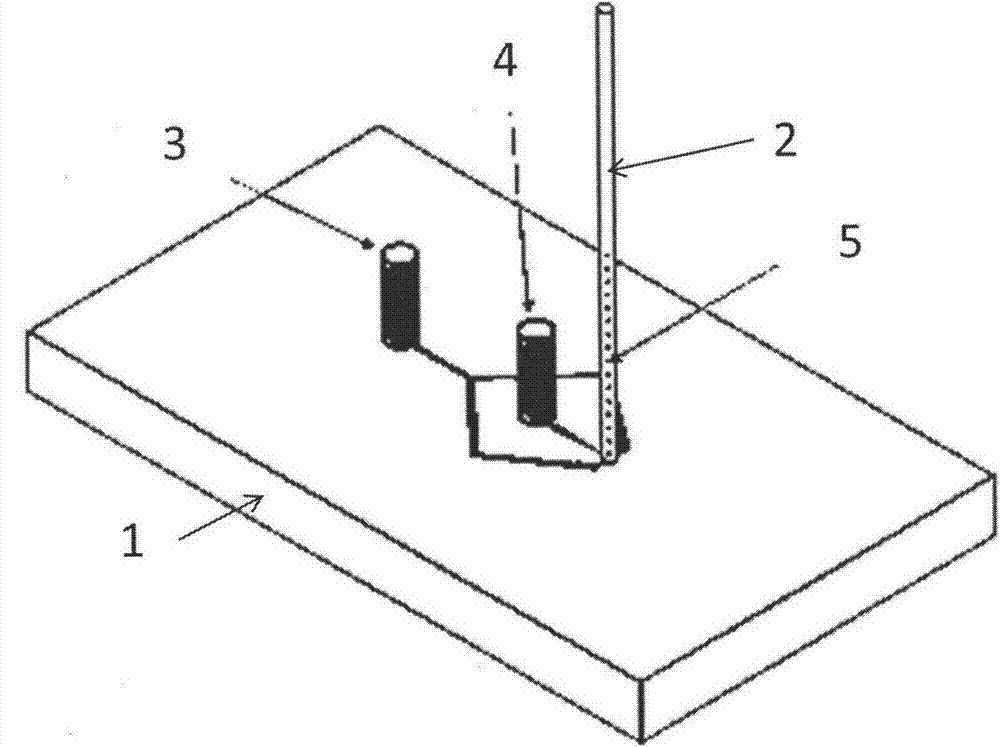
[0028] see figure 1 , the preparation steps of the water-in-oil droplet capillary microfluidic chip are as follows:
[0029] 1. Fabrication of the mask: first design and draw the microstructure and microchannel graphics of the droplet-generating capillary microfluidic chip with the design software (AutoCAD), and print the graphics into a mask, and use the mask to make a silicon wafer mold;
[0030] 2. Silicon wafer mold making: first clean the silicon wafer, and use concentrated H 2 SO 4 / H 2 o 2 =3:1, soak for 15min, then clean the wafer with absolute ethanol, acetone, and ultrapure water; dry the wafer on a heating plate; modify the wafer with hexamethyldisilazane, pour the photoresist AZ-50XT, drop glue at 2000rpm for 1min15s, then carry out pre-baking polymerization; place the mask and silicon wafer in the corresponding position of the photolithography machine, UV exposure, and finally develop;
[0031] 3. Fabrication of PDMS chips: use the prepared silicon wafer mold...
Embodiment 2
[0038] The preparation steps of capillary microfluidic chip for oil-in-water droplet generation are as follows:
[0039]1. Fabrication of the mask: first design and draw the microstructure and microchannel graphics of the droplet-generating capillary microfluidic chip with the design software (AutoCAD), and print the graphics into a mask, and use the mask to make a silicon wafer mold;
[0040] 2. Cleaning of glass substrate: use concentrated H 2 SO 4 / H 2 o 2 = 3:1, soak for 15min, then clean the wafer with absolute ethanol, acetone, and ultrapure water, and dry it on a heating plate;
[0041] 3. Sacrificial layer sputtering: Sputter a chromium layer with a thickness of 145nm on the surface of the cleaned glass substrate with an ion sputtering device;
[0042] 4. Pre-treatment of photolithography: After modifying the glass substrate with hexamethyldisilazane on the chromium plate glass, pour the photoresist AZ-4620, drop the glue at 3000rpm for 1min, and then carry out pre...
PUM
| Property | Measurement | Unit |
|---|---|---|
| Thickness | aaaaa | aaaaa |
| Side length | aaaaa | aaaaa |
| Width | aaaaa | aaaaa |
Abstract
Description
Claims
Application Information
 - R&D
- Intellectual Property
- Life Sciences
- Materials
- Tech Scout
- Unparalleled Data Quality
- Higher Quality Content
- 60% Fewer Hallucinations
Browse by: Latest US Patents, China's latest patents, Technical Efficacy Thesaurus, Application Domain, Technology Topic, Popular Technical Reports.
© 2025 PatSnap. All rights reserved.Legal|Privacy policy|Modern Slavery Act Transparency Statement|Sitemap|About US| Contact US: help@patsnap.com


