Organic light-emitting device and method for manufacturing same
An electroluminescent device and electroluminescent technology, which are applied in the directions of organic light-emitting device, organic light-emitting device manufacturing/processing, organic light-emitting device structure, etc., can solve the problems of complex manufacturing cost of supporting equipment, poor water and oxygen resistance, and expensive raw materials, etc. To achieve the effect of improving waterproof and oxygen resistance, preventing cracks and good stability
- Summary
- Abstract
- Description
- Claims
- Application Information
AI Technical Summary
Problems solved by technology
Method used
Image

Examples
preparation example Construction
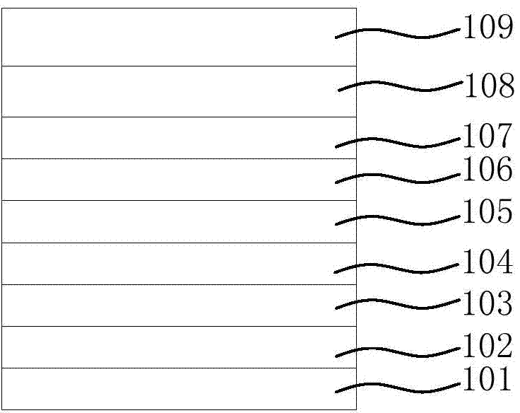
[0051] The method for preparing the above-mentioned organic electroluminescent device specifically includes the following steps:
[0052] (a) on the anode conductive layer of the cleaned anode conductive substrate, the method of vacuum evaporation is used to sequentially stack and prepare a hole injection layer, a hole transport layer, a light-emitting layer, an electron transport layer, an electron injection layer and a cathode layer;
[0053] (b) On the cathode layer, first, prepare an organic barrier layer by vacuum evaporation; then prepare a hybrid barrier layer on the mixed barrier layer by magnetron sputtering; then, alternately stack several times to prepare Organic barrier layers and hybrid barrier layers; wherein,
[0054] The material of the organic barrier layer is copper phthalocyanine, N,N'-diphenyl-N,N'-di(1-naphthyl)-1,1'-biphenyl-4,4'-diamine, 8-Hydroxyquinoline aluminum, 4,4',4''-tris(N-3-methylphenyl-N-phenylamino)triphenylamine or 4,7-diphenyl-1,10-phenant...
Embodiment 1
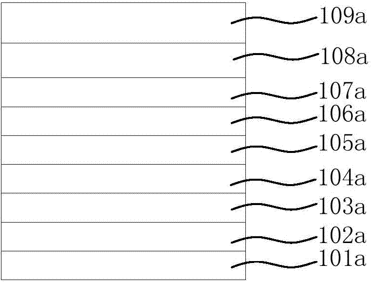
[0062] Such as Figure 1A As shown, in the organic electroluminescence device of the present embodiment 1, the anode conductive substrate is an ITO glass substrate 101a, and the hole injection layer is MoO 3 : NPB layer 102a, hole transport layer is TCTA layer 103a, light emitting layer is TPBI: Ir(ppy) 3 layer 104a, electron transport layer is Bphen layer 105a, electron injection layer is CsN 3 : Bphen layer 106a, cathode layer is Al layer 107a, organic barrier layer is CuPc layer 108a, mixed barrier layer is tris(3-methylbutyl)gallium (structural formula is as follows): MoO 3 Layer 109a, where the colon ":" indicates mutual doping, and the structural formula of tris(3-methylbutyl)gallium is as follows (P1):
[0063]
[0064] The above-mentioned organic electroluminescent device is prepared according to the following steps:
[0065] Step S1, pretreatment of the anode conductive substrate 101a: use the ITO glass substrate 101a as the anode conductive substrate, and first...
Embodiment 2
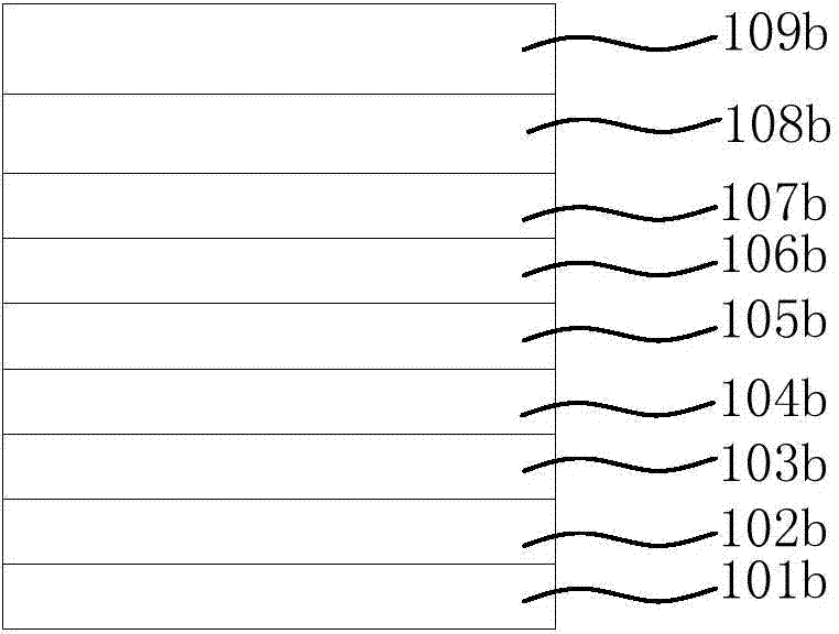
[0077] Such as Figure 1B As shown, in the organic electroluminescence device of the present embodiment 2, the anode conductive substrate is an ITO glass substrate 101b, and the hole injection layer is MoO 3 : NPB layer 102b, hole transport layer is TCTA layer 103b, light emitting layer is TPBI: Ir(ppy) 3 Layer 104b, electron transport layer is Bphen layer 105b, electron injection layer is CsN 3 : Bphen layer 106b, cathode layer is Al layer 107b, organic barrier layer is CuPc layer 108b, mixed barrier layer is tris(3,7-dimethyloctyl)gallium (structural formula is as follows): V 2 o 5 Layer 109b, where the colon ":" indicates mutual doping, and the structural formula of tris(3,7-dimethyloctyl)gallium is as follows (P2):
[0078]
[0079] The above-mentioned organic electroluminescent device is prepared according to the following steps:
[0080] The above-mentioned organic electroluminescent device is prepared according to the following steps:
[0081] Step S1~step S7 ar...
PUM
| Property | Measurement | Unit |
|---|---|---|
| Thickness | aaaaa | aaaaa |
| Thickness | aaaaa | aaaaa |
| Thickness | aaaaa | aaaaa |
Abstract
Description
Claims
Application Information
 - R&D
- Intellectual Property
- Life Sciences
- Materials
- Tech Scout
- Unparalleled Data Quality
- Higher Quality Content
- 60% Fewer Hallucinations
Browse by: Latest US Patents, China's latest patents, Technical Efficacy Thesaurus, Application Domain, Technology Topic, Popular Technical Reports.
© 2025 PatSnap. All rights reserved.Legal|Privacy policy|Modern Slavery Act Transparency Statement|Sitemap|About US| Contact US: help@patsnap.com