Supercharge Your Innovation With Domain-Expert AI Agents!

Organic light-emitting device and preparation method thereof

An electroluminescent device, electroluminescent technology, applied in the direction of electric solid device, semiconductor/solid state device manufacturing, electrical components, etc., can solve the problems of short service life, poor mechanical strength and high cost

Inactive Publication Date: 2015-04-15
OCEANS KING LIGHTING SCI&TECH CO LTD +2
View PDF0 Cites 0 Cited by
  • Summary
  • Abstract
  • Description
  • Claims
  • Application Information

AI Technical Summary

Problems solved by technology

[0004] For OLED products, if the traditional OLED packaging technology is used, adding a packaging cover on the back of the device will cause problems such as heavy weight, high cost, and poor mechanical strength, which will limit the performance of OLED products.
At present, most OLEDs are not waterproof and oxygen-resistant, and have a short service life. The preparation process is complicated and the cost is high.

Method used


Image

  • Organic light-emitting device and preparation method thereof
  • Organic light-emitting device and preparation method thereof

Examples


Embodiment 1

[0083] An organic electroluminescent device is prepared through the following steps:

[0084] (1) Provide a clean anode conductive substrate:

[0085] Clean the ITO glass substrate with acetone, ethanol, deionized water, and ethanol in an ultrasonic cleaner in sequence, wash and wash for 5 minutes in one item, then blow dry with nitrogen, and dry in an oven for later use; surface activation of the cleaned ITO glass processing; ITO thickness is 100nm;

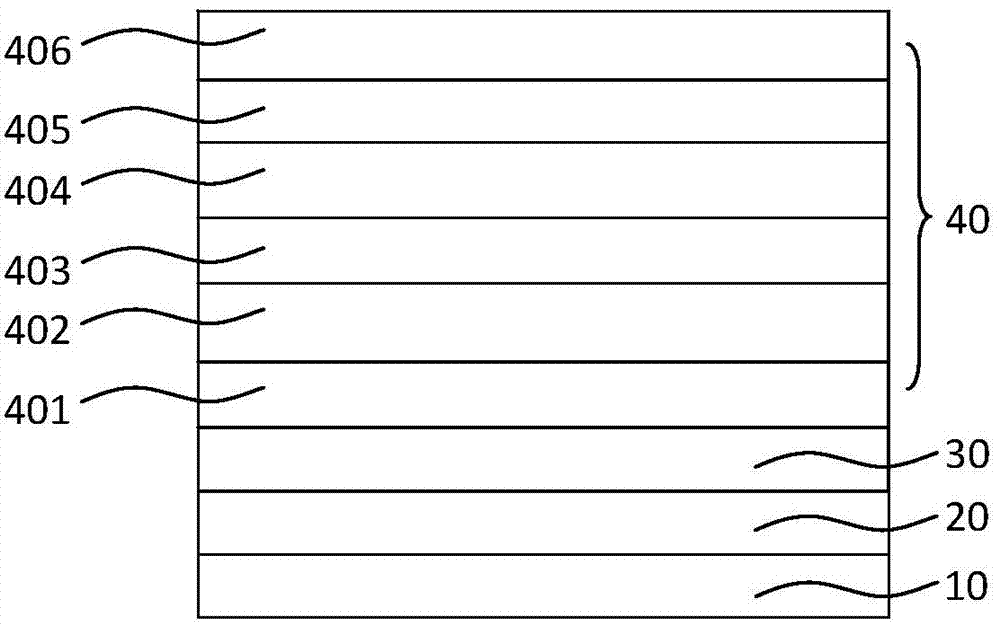
[0086] (2) Vacuum evaporation of the luminescent functional layer on the ITO glass substrate:

[0087] Specifically, the light emitting functional layer includes a hole injection layer, a hole transport layer, a light emitting layer, an electron transport layer and an electron injection layer;

[0088] Preparation of the hole injection layer: The mixture obtained by mixing MoO3 and NPB according to the mass ratio of 1:3 is used as the material of the hole injection layer, the thickness is 10nm, and the vacuum degree is 3×10 -...

Embodiment 2

[0106] An organic electroluminescent device is prepared through the following steps:

[0107] (1), (2), (3) are the same as embodiment 1;

[0108] (4) Prepare the encapsulation layer on the outside of the cathode:

[0109] The encapsulation layer is an alternately laminated silicon oxycarbide barrier layer and an inorganic barrier layer;

[0110] Fabrication of silicon oxycarbide barrier layer: with TMS as the source, N 2 A mixed gas of O and Ar was used to prepare a silicon oxycarbide film in a PECVD deposition chamber to obtain a silicon oxycarbide barrier layer. The preparation process conditions were a TMS flow rate of 25 sccm, a mixed gas flow rate of 50 sccm, and N 2 The volume fraction of O in the mixed gas is 60%, and the thickness of the silicon oxycarbide film produced is 280nm;

[0111] Fabrication of the inorganic barrier layer: the organic electroluminescent device sample prepared with the silicon oxycarbide barrier layer was placed in the deposition chamber of...

Embodiment 3

[0119] An organic electroluminescent device is prepared through the following steps:

[0120] (1), (2), (3) are the same as embodiment 1;

[0121] (4) Prepare the encapsulation layer on the outside of the cathode:

[0122] The encapsulation layer is an alternately laminated silicon oxycarbide barrier layer and an inorganic barrier layer;

[0123] Fabrication of silicon oxycarbide barrier layer: using TEOS as the source, passing through N 2 A mixed gas of O and Ar was used to prepare a silicon oxycarbide film in a PECVD deposition chamber to obtain a silicon oxycarbide barrier layer. The preparation process conditions were TEOS flow rate of 20 sccm, mixed gas flow rate of 20 sccm, N 2 The volume fraction of O in the mixed gas is 40%, and the thickness of the silicon oxycarbide film produced is 250nm;

[0124] Fabrication of the inorganic barrier layer: the organic electroluminescent device sample prepared with the silicon oxycarbide barrier layer was placed in the deposition...


PUM

PropertyMeasurementUnit
thicknessaaaaaaaaaa
thicknessaaaaaaaaaa
thicknessaaaaaaaaaa

Abstract

The invention aims to provide an organic light-emitting device with a packaging layer structure. The packaging layer is composed of silicon oxynitride barrier layers and inorganic barrier layers which are alternately stacked, wherein the silicon oxynitride barrier layers are made of silicon oxynitride, and the inorganic barrier layers are made of B2O3, Al2O3, Ga2O3, In2O3 or Tl2O3. The packaging layer can effectively prevent the erosion of external water, oxygen and other active substances to the organic light-emitting device and prolong the service life of the organic light-emitting device. The invention further provides a preparation method of the organic light-emitting device. The preparation method has the advantages of simple process, cheap raw materials and easy realization of large-area preparation.

Description

technical field [0001] The invention relates to the field of organic electroluminescence, in particular to an organic electroluminescence device and a preparation method thereof. Background technique [0002] An organic electroluminescent device (OLED) is an energy conversion device that uses organic materials as light-emitting materials and can convert applied electrical energy into light energy. It has outstanding performances such as ultra-thin, self-luminous, fast response, low power consumption, etc., and has extremely broad application prospects in display, lighting and other fields. [0003] Organic electroluminescent materials are particularly sensitive to oxygen and moisture intrusion. On the one hand, because oxygen is a quencher, the quantum efficiency of luminescence will be significantly reduced, and the oxidation of oxygen to the hole transport layer will also reduce its transport ability; on the other hand, water vapor will hydrolyze organic compounds, making...

Claims


Application Information

Patent Timeline
Patent Type & Authority Applications(China)
IPC IPC(8): H01L51/52H01L51/54H01L51/56
CPCH10K50/84H10K71/00
Inventor 周明杰钟铁涛王平张振华
Owner OCEANS KING LIGHTING SCI&TECH CO LTD
Features
  • R&D
  • Intellectual Property
  • Life Sciences
  • Materials
  • Tech Scout
  • Unparalleled Data Quality
  • Higher Quality Content
  • 60% Fewer Hallucinations
Learn More