Organic electroluminescent device and its preparation method
An electroluminescent device and luminescent technology, which is applied in the direction of electric solid-state devices, semiconductor/solid-state device manufacturing, electrical components, etc., can solve problems such as failure of organic functional materials, degradation of electrode performance, and impact on device life, so as to improve effective protection , The preparation process is simple, and the effect of easy large-area preparation
- Summary
- Abstract
- Description
- Claims
- Application Information
AI Technical Summary
Problems solved by technology
Method used
Image

Examples
preparation example Construction
[0036]The preparation method of the organic electroluminescent device of the present invention comprises the following steps:
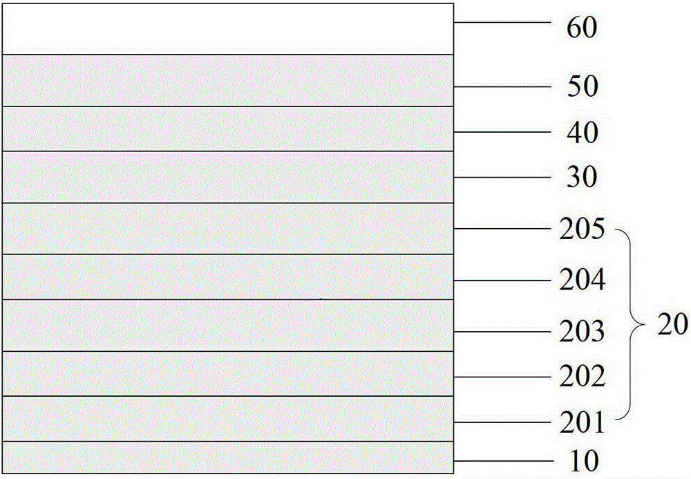
[0037] S1, on the surface of the anode layer of the anode substrate 10, the vacuum evaporation functional layer 20 (hole injection layer 201, hole transport layer 202, light emitting layer 203, electron transport layer 204, electron injection layer 205) and cathode layer 30 are laminated in sequence;
[0038] S2. Vacuum-deposit an organic barrier layer 40 on the cathode layer 30; wherein, the material of the organic barrier layer 40 is copper phthalocyanine (CuPc), N,N'-diphenyl-N,N'-diphenyl (1-naphthyl)-1,1'-biphenyl-4,4'-diamine (NPB), 8-hydroxyquinoline aluminum (Alq3), 4,4',4"-tri(N-3- Methylphenyl-N-phenylamino)triphenylamine (m-MTDATA) or 4,7-diphenyl-1,10-phenanthroline (BCP); in the vacuum evaporation, the degree of vacuum is 1 ×10 -5 Pa-1×10 -3 Pa, the evaporation rate is
[0039] S3. Put the sample, fluoride and metal phthalocyanine c...
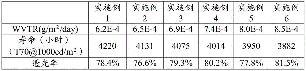
Embodiment 1
[0046] Embodiment 1 organic electroluminescent device
[0047] include:
[0048] (1) Anode base;
[0049] (2) Functional layer, located between the anode substrate and the cathode layer, comprising a hole injection layer, a hole transport layer, a light-emitting layer, an electron transport layer and an electron injection layer stacked in sequence, and the hole injection layer is located at the anode on the base;
[0050] (3) cathode layer;
[0051] (4) An organic barrier layer, vapor-deposited on the cathode layer; the material of the organic barrier layer is CuPc, and the organic barrier layer is 6 layers, and the thickness of each layer is 300nm;
[0052] (5) Inorganic barrier layer, vapor-deposited on the organic barrier layer; the material of the inorganic barrier layer is a mixture of LiF doped with 20wt% CuPc; the inorganic barrier layer has 6 layers, and the thickness of each layer is 250nm.
[0053] The organic barrier layer and the inorganic barrier layer are eva...
Embodiment 2
[0079] Embodiment 2 organic electroluminescence device
[0080] include:
[0081] (1) anode base; with embodiment 1;
[0082] (2) functional layer; with embodiment 1;
[0083] (3) cathode layer; with embodiment 1;
[0084] (4) An organic barrier layer, vapor-deposited on the cathode layer; the material of the organic barrier layer is NPB, and the organic barrier layer is 5 layers, and the thickness of each layer is 250nm;
[0085] (5) Inorganic barrier layer, vapor-deposited on the organic barrier layer, the material of the inorganic barrier layer is CeF doped with 30wt% ZnPc 2 Composed mixture, the inorganic barrier layer is 5 layers, and the thickness of each layer is 300nm.
[0086] The organic barrier layer and the inorganic barrier layer are evaporated alternately.
[0087] The above (1)-(5) constitute an organic electroluminescent device.
[0088] (6) PET film, encapsulating the above-mentioned organic electroluminescent device in the PET film and the anode substra...
PUM
 Abstract
Description
Claims
Application Information