

Terahertz quantum cascade laser device structure and production method thereof
A technology of quantum cascade and device structure, applied in laser parts, lasers, phonon exciters, etc., can solve problems such as poor heat dissipation, and achieve the effect of improving heat dissipation and strong heat dissipation.
- Summary
- Abstract
- Description
- Claims
- Application Information
AI Technical Summary
Problems solved by technology
Method used
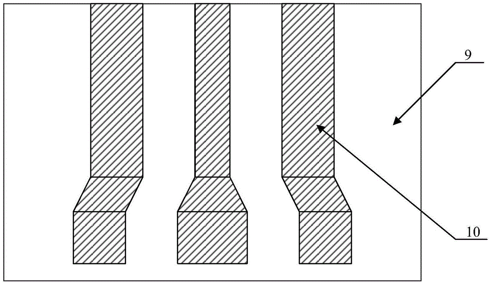
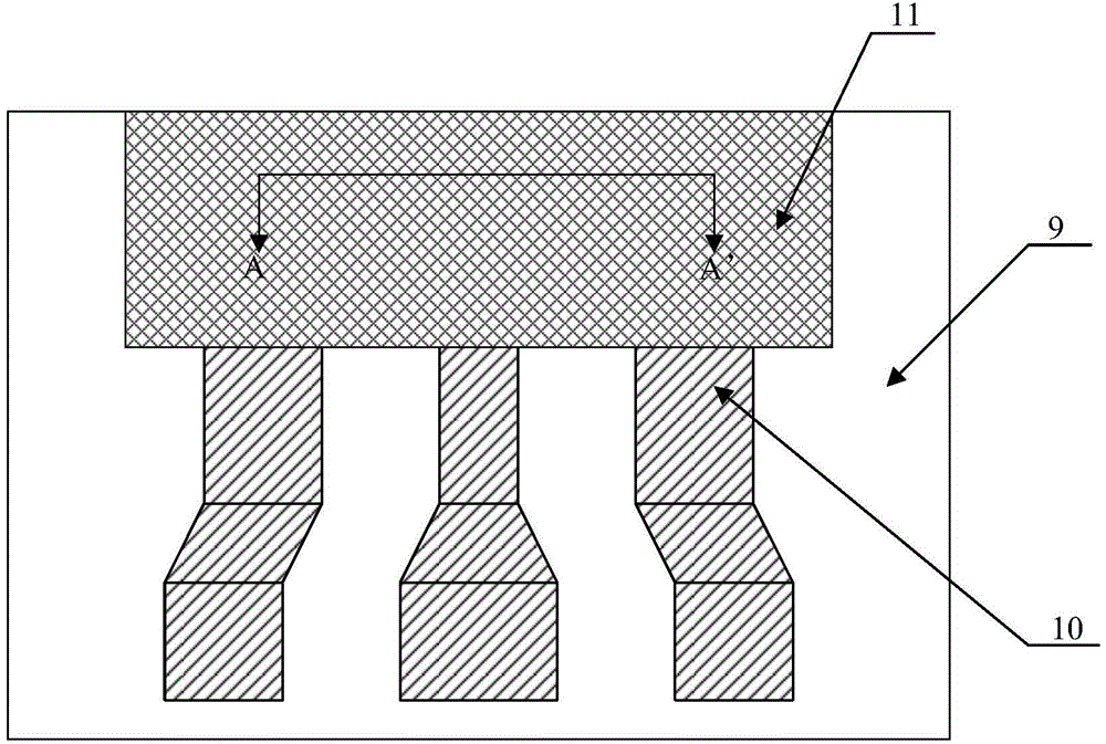
Image

Examples
Embodiment 1
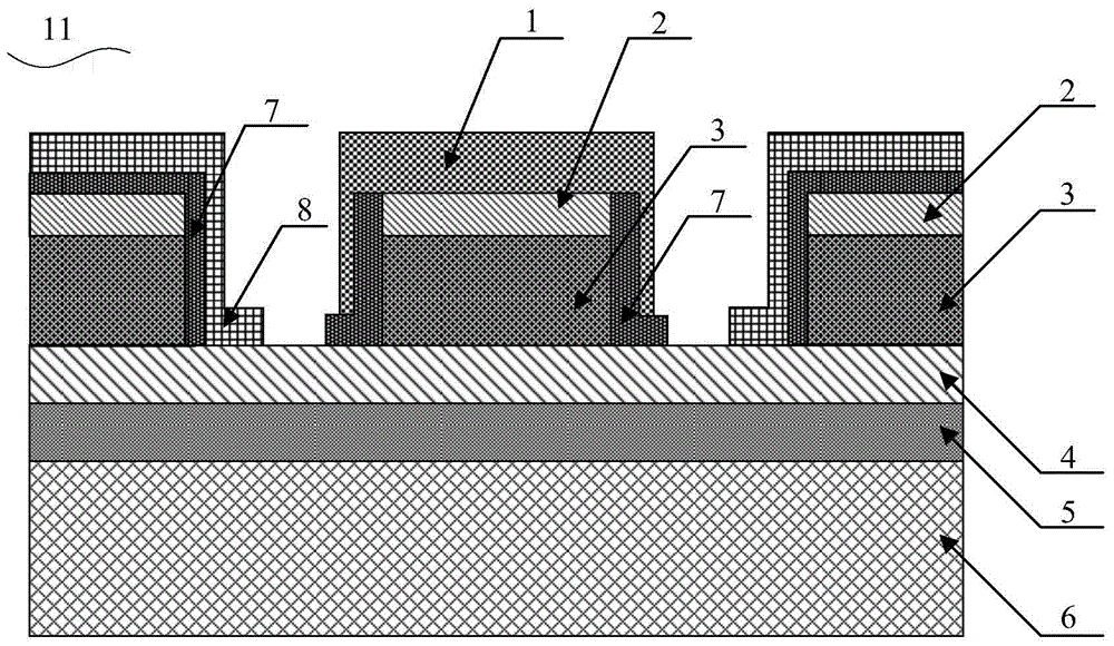
[0045] see figure 1 , the present invention provides a terahertz quantum cascade laser device structure, the terahertz quantum cascade laser device structure at least includes: a ridge waveguide structure 11; the ridge waveguide structure 11 includes a semi-insulating GaAs substrate 6, a GaAs buffer layer 5. Lower contact layer 4, active region 3, upper contact layer 2, thermally conductive insulating layer 7, upper metal layer 1 (ie, upper electrode) and lower metal layer 8 (ie, lower electrode); wherein, the semi-insulating GaAs lining The bottom 6, the GaAs buffer layer 5, the lower contact layer 4, the active region 3 and the upper contact layer 2 are stacked sequentially from bottom to top, and the active region 3 and the upper contact layer 2 are formed on the lower contact layer 4 Ridge structure; the upper metal layer 1 covers the top and both sides of the ridge structure; the thermally conductive insulating layer 7 is located on both sides of the ridge structure, and ...
Embodiment 2
[0063] This embodiment also provides a method for fabricating a terahertz quantum cascade laser device structure, such as Figure 5 As shown, the manufacturing method of the terahertz quantum cascade laser device structure includes the following steps:
[0064] Step 1: growing a buffer layer, a heavily n-type doped lower contact layer, an active region, and an n-type heavily doped upper contact layer on a semi-insulating GaAs substrate;
[0065] Step 2: For the first photolithography, the ridge waveguide is etched by a dry or wet etching process to form a ridge waveguide structure and a lower electrode support structure;
[0066] Step 3: growing a thermally conductive insulating layer on the ridge waveguide structure and the lower electrode supporting structure by plasma-enhanced chemical vapor deposition (PECVD), the material of the thermally conductive insulating layer is preferably silicon, and the thermally conductive insulating layer The thickness of the upper electrode ...
PUM
| Property | Measurement | Unit |
|---|---|---|
| Thickness | aaaaa | aaaaa |
Abstract
Description
Claims
Application Information