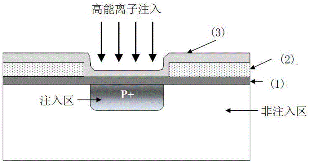
Composite mask for high-energy ion implantation
A composite mask, high-energy ion technology, applied in the field of mask, can solve the problems of easy residual photoresist mask, large pattern size process error, affecting the blocking effect of thin film mask, etc., so as to avoid device process failure, The effect of avoiding the easy residue of the mask and shortening the degumming time
- Summary
- Abstract
- Description
- Claims
- Application Information
AI Technical Summary
Problems solved by technology
Method used
Image
Examples
Embodiment 1
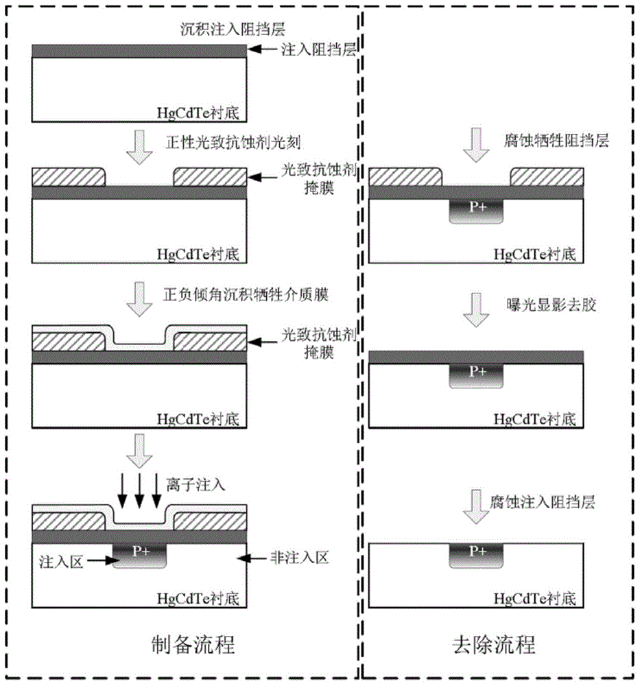
[0024] Using the mask preparation method described in the present invention, evaporation deposition, photolithography, and positive and negative inclination angle evaporation deposition are carried out on the surface of the mercury cadmium telluride epitaxial material chip. The preparation process is shown in the attached figure 2 shown. Firstly, a cadmium telluride injection barrier layer with a thickness of ~60nm is deposited by thermal evaporation on the surface of the HgCdTe epitaxial material chip after annealing treatment and surface corrosion treatment, the chip is cleaned, and a layer of 2-3 microns in thickness is spin-coated on the chip surface A thick positive photoresist is used to expose the chip to ultraviolet light with a photolithography plate, and after developing and fixing, a photoresist injection mask is obtained.
[0025] Load the chip with the mask pattern prepared on the sample stage of the high-vacuum thermal evaporation equipment, first rotate the sam...
Embodiment 2
[0029] Using the mask preparation method described in the present invention, evaporation deposition, photolithography, and positive and negative inclination angle sputter deposition are carried out on the surface of the mercury cadmium telluride epitaxial material chip. The preparation process is shown in the attached figure 2 shown. First, thermally evaporate and deposit ~20nm thick cadmium telluride implant barrier layer on the surface of the HgCdTe epitaxial material chip after annealing treatment and surface corrosion treatment, clean the chip, and spin coat a layer of 2-3 microns in thickness on the chip surface A thick positive photoresist is used to expose the chip to ultraviolet light with a photolithography plate, and after developing and fixing, a photoresist injection mask is obtained.
[0030] Load the chip with the prepared mask pattern on the sample stage of the magnetron sputtering equipment, first rotate the sample stage at an inclination angle of 0°, and sput...
Embodiment 3
[0034] Using the mask preparation method described in the present invention, evaporation deposition, photolithography, and positive and negative inclination angle evaporation deposition are carried out on the surface of the mercury cadmium telluride epitaxial material chip. The preparation process is shown in the attached figure 2 shown. First, thermally evaporate and deposit ~200nm thick cadmium telluride implant barrier layer on the surface of the HgCdTe epitaxial material chip after annealing treatment and surface corrosion treatment, clean the chip, and spin coat a layer of 2-3 microns in thickness on the chip surface A thick positive photoresist is used to expose the chip to ultraviolet light with a photolithography plate, and after developing and fixing, a photoresist injection mask is obtained.
[0035] Load the chip with the prepared mask pattern on the sample stage of the high-vacuum thermal evaporation equipment, first rotate the sample stage at an inclination angle...
PUM
 Abstract
Description
Claims
Application Information
 - R&D
- Intellectual Property
- Life Sciences
- Materials
- Tech Scout
- Unparalleled Data Quality
- Higher Quality Content
- 60% Fewer Hallucinations
Browse by: Latest US Patents, China's latest patents, Technical Efficacy Thesaurus, Application Domain, Technology Topic, Popular Technical Reports.
© 2025 PatSnap. All rights reserved.Legal|Privacy policy|Modern Slavery Act Transparency Statement|Sitemap|About US| Contact US: help@patsnap.com


