Crystalline silicon and silicon film composite type unijunction PIN solar cell with transition layers and preparation method for crystalline silicon and silicon film composite type unijunction PIN solar cell

A solar cell and transition layer technology, which is applied in circuits, photovoltaic power generation, electrical components, etc., can solve the problems that no one has developed a single-junction PIN solar cell manufacturing method, and no one has developed a thin-film solar cell manufacturing technology.

Active Publication Date: 2015-04-29
湖南共创光伏科技有限公司
View PDF6 Cites 0 Cited by
  • Summary
  • Abstract
  • Description
  • Claims
  • Application Information

AI Technical Summary

Problems solved by technology

However, before the patent number ZL200910044772.4, no one has used a series of six materials with different energy gaps to form a thin-film solar cell with a single-junction multi-layer PIN structure, and no one has developed and prepared th

Method used


Image

  • Crystalline silicon and silicon film composite type unijunction PIN solar cell with transition layers and preparation method for crystalline silicon and silicon film composite type unijunction PIN solar cell
  • Crystalline silicon and silicon film composite type unijunction PIN solar cell with transition layers and preparation method for crystalline silicon and silicon film composite type unijunction PIN solar cell
  • Crystalline silicon and silicon film composite type unijunction PIN solar cell with transition layers and preparation method for crystalline silicon and silicon film composite type unijunction PIN solar cell

Examples


Embodiment 1

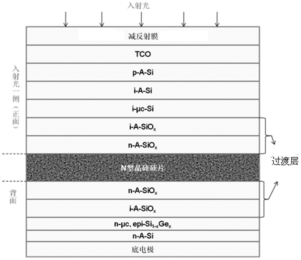
[0077] A kind of crystalline silicon and silicon thin film composite type single-junction PIN solar cell with transition layer, comprises n-type silicon wafer, is characterized in that, on the front surface of n-type silicon wafer or on the back surface of n-type silicon wafer or on n-type silicon wafer The front surface and the back surface of the silicon wafer are provided with a transition layer; the transition layer is one or more layers, any one of which is a silicon-rich silicon oxide layer; the silicon-rich silicon oxide layer is selected from i-A-SiO x , i-μc-SiO x , n-A-SiO x , n-μc-SiO x Any of the above, wherein 0≤x≤2; or the silicon-rich silicon oxide layer is selected from n-type gradient μc-SiO x and n-type gradient A-SiO x , where 0≤x≤2, the "gradient" means: by changing the value of x in the silicon-rich silicon oxide gradually changes from 2 to 0, while the silicon oxide changes from silicon oxide——to silicon-rich silicon oxide layer— — then change to the ...

Embodiment 2

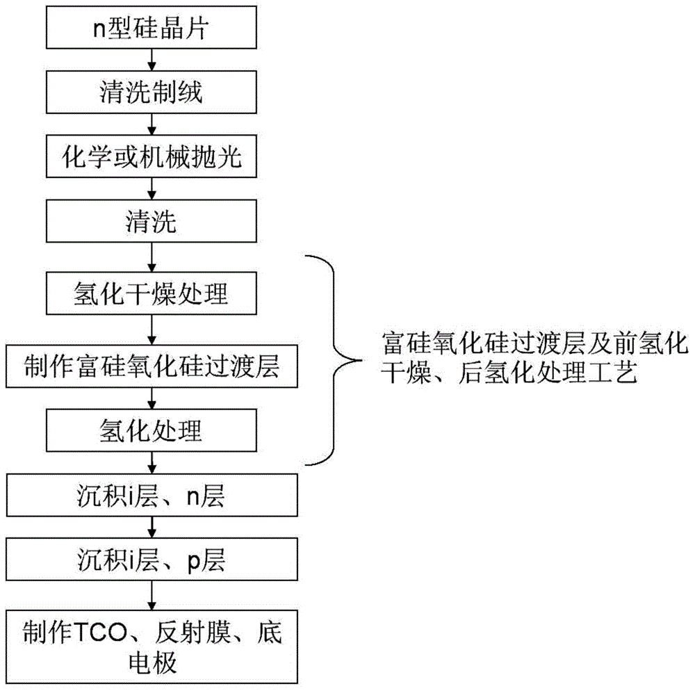
[0080] The manufacturing method of the transition layer, such as figure 2 shown, including the following methods:

[0081] The first type: After preliminary cleaning, chemical texturing, chemical or mechanical double-sided polishing of the n-type silicon wafer, the n-type silicon wafer is cleaned again, and the cleaned silicon wafer is pre-hydrogenated and dried. The treatment method is as follows: : Send the silicon wafer to the equipment with a closed chamber, evacuate the atmosphere until the chamber pressure is less than or equal to (≤) 1Pascal; the chamber temperature is controlled between 30°C and 350°C, and hydrogen or a mixture of hydrogen and nitrogen is introduced gas; dry silicon wafers under a hydrogen atmosphere. The purity of hydrogen and nitrogen is greater than or equal to (≥) 99.99%; if a mixed gas is used, the volume ratio of hydrogen and nitrogen is 0.1 to 100 times; the hydrogenation drying time is 1 to 60 minutes. Send the hydrogenated and dried silicon...


PUM

PropertyMeasurementUnit
Thicknessaaaaaaaaaa

Abstract

The invention provides a crystalline silicon and silicon film composite type unijunction PIN solar cell with transition layers and a preparation method for the crystalline silicon and silicon film composite type unijunction PIN solar cell. The solar cell is provided with one or more transition layers on the front surface of an n-type silicon wafer, the back surface of the n-type silicon wafer or both the front surface and the back surface of the n-type silicon wafer, and any transmission layer is a silicon-rich silicon oxide layer. The preparation method for the crystalline silicon and silicon film composite type unijunction PIN solar cell comprises the following steps: after finishing texturing, polishing and cleaning of the silicon wafer, adding a pre-hydrogenation drying process, and after finishing a process of the transition layers, adding a post-hydrogenation drying process; the two methods are used for improving the interface quality and the structure stability. The cell conversion efficiency of the crystalline silicon film composite cell adopting the transition layers and subjected to the pre-hydrogenation drying process and the post-hydrogenation drying process can be improved by more than 10% in comparison with that of an original cell.

Description

technical field [0001] The invention relates to crystalline silicon and thin film composite solar cells, in particular to the structural design and manufacturing method of crystalline silicon and silicon thin film composite single-junction PIN solar cells with a transition layer structure. Background technique [0002] Since the French scientist AE. Becquerel discovered the photoelectric conversion phenomenon in 1839, the first solar cell based on semiconductor selenium was born in 1883. RuSSell obtained the first solar cell patent (US.2,402,662) in 1946, and its photoelectric conversion efficiency was only 1%. It was not until 1954 that Bell Laboratories' research discovered that doped silicon-based materials have high photoelectric conversion efficiency. This research laid the foundation for the modern solar cell industry. In 1958, the Haffman Power Company of the United States installed the first solar panel on a satellite in the United States, and its photoelectric con...

Claims


Application Information

Patent Timeline
IPC IPC(8): H01L31/075H01L31/18
CPCH01L31/077H01L31/18Y02E10/547Y02E10/548Y02P70/50
Inventor 何湘衡李廷凯
Owner 湖南共创光伏科技有限公司
Why Eureka
Try Eureka