High-efficiency passivated contact crystalline silicon solar cell and preparation method thereof

A solar cell, crystalline silicon technology, applied in circuits, photovoltaic power generation, electrical components, etc., can solve the problems of reducing the bulk resistivity filling factor of silicon wafers, high bulk resistivity of silicon wafers, limiting open circuit voltage, etc. Efficiency, reducing bulk resistivity, and improving photoelectric efficiency

Inactive Publication Date: 2019-08-30
TRINA SOLAR CO LTD
View PDF6 Cites 2 Cited by
  • Summary
  • Abstract
  • Description
  • Claims
  • Application Information

AI Technical Summary

Problems solved by technology

The passivation contact technology uses silicon oxide and doped polysilicon film as the passivation layer, which can form a good passivation effect. However, due to the thick silicon wafers used in mass production in the industry, the volume resistivity of the silicon wafer itself The filling factor is reduced, and the defect state in the silicon substrate also limits the further improvement of the open circuit voltage
[0003] The current solution mainly removes the defect state of the silicon wafer substrate by chemical liquid cleaning and optimizes the screen printing paste to improve the open circuit voltage and fill factor. Although the current solution improves the open circuit voltage and fill factor, it cannot Fundamentally solve the problem of high bulk resistivity of silicon wafers

Method used


Image

  • High-efficiency passivated contact crystalline silicon solar cell and preparation method thereof
  • High-efficiency passivated contact crystalline silicon solar cell and preparation method thereof

Examples


Embodiment 1

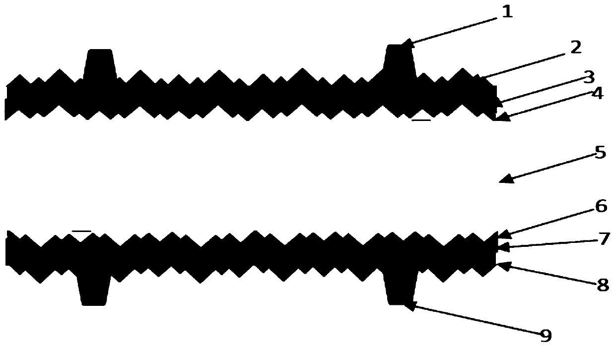
[0029] A method for preparing an alkali-etched ultra-thin N-type passivated contact crystalline silicon solar cell, comprising the steps of:

[0030] Using N-type monocrystalline silicon as the silicon substrate, first perform conventional cleaning and then use a TMAH solution with a volume concentration of 20% to thin the cleaned silicon wafer, and the process time is 650s.

[0031] The thinned silicon wafer is textured and boron diffused. After the diffusion is completed, the BSG on the back is removed on one side, and then the single-sided texturing process on the back is adopted. Then deposit a layer of 5-15nm silicon oxide layer and 150-250nm intrinsic polysilicon layer on the back side, the deposition method is PECVD.

[0032] This is followed by phosphorus diffusion, followed by dehydration of the silicon wafer, followed by deposition of aluminum oxide and silicon nitride on the front side of the silicon wafer, and silicon nitride on the back side.

[0033] Finally, sc...


PUM

PropertyMeasurementUnit
thicknessaaaaaaaaaa
thicknessaaaaaaaaaa

Abstract

The invention discloses a high-efficiency passivated contact crystalline silicon solar cell and a preparation method thereof. The method comprises the following steps of preprocessing and thinning a silicon wafer: conventionally cleaning the silicon wafer and then thinning the silicon wafer by using a TMAH alkali solution having a concentration of 10-30%; texturing: conventionally texturing the silicon wafer; diffusion: performing conventional boron diffusion on the silicon wafer; removing a borosilicate glass layer on the back side of the silicon wafer; texturing the back side of the siliconwafer and then depositing a silicon oxide layer on the back side of the silicon wafer; depositing a polycrystalline silicon film on the silicon oxide layer on the back side of the silicon wafer; cleaning the silicon wafer with HF, then depositing an aluminum oxide film and a silicon nitride film on the front side of the silicon wafer, and depositing a silicon nitride film on the back side of the silicon wafer; and silk printing a front side electrode and a back side electrode. In order to fundamentally solve the low fill factor due to high volume resistivity, the method directly thins the silicon wafer by alkali solution corrosion in large-scale production, thereby significantly increasing the fill factor of the battery and thus improving photoelectric conversion efficiency.

Description

technical field [0001] The invention belongs to the technical field of photovoltaics, and in particular relates to a high-efficiency passivation contact crystalline silicon solar cell and a preparation method thereof. Background technique [0002] Pursuing to improve battery conversion efficiency while reducing or even maintaining manufacturing costs is the goal that the industry is constantly pursuing and where it needs to improve its own competitiveness. In terms of high-efficiency batteries, many foreign scientific research institutes and enterprises have carried out a lot of research and developed many high-efficiency batteries with new structures. Passivated contact cells have become a hot research topic at present. Its highest efficiency reaches 26.1%, which was created by the famous German Fraunhofer ISE Institute. The passivation contact technology uses silicon oxide and doped polysilicon film as the passivation layer, which can form a good passivation effect. Howev...

Claims


Application Information

Patent Timeline
Patent Type & Authority Applications(China)
IPC IPC(8): H01L31/18H01L31/068
CPCH01L31/068H01L31/1804H01L31/1868Y02E10/546Y02E10/547Y02P70/50
Inventor 王尧何宇刘成法陈达明陈奕峰邹杨夏锐林文杰袁玲龚剑
Owner TRINA SOLAR CO LTD
Why Eureka
Try Eureka