Organic electroluminescent device and manufacturing method thereof

An electroluminescence device and luminescence technology, applied in organic light-emitting devices, organic light-emitting device structures, organic semiconductor devices, etc., can solve the problems of low cathode luminescence brightness, low cathode, and inconsistent luminance brightness of the light-emitting surface, etc.

Inactive Publication Date: 2015-04-29
OCEANS KING LIGHTING SCI&TECH CO LTD +2
View PDF0 Cites 4 Cited by
  • Summary
  • Abstract
  • Description
  • Claims
  • Application Information

AI Technical Summary

Problems solved by technology

However, in current double-sided light-emitting devices, the anode usually uses an ITO conductive film, and the cathode uses a thin layer of metal, such as Ag, etc., but the transmittance of the cathode is significantly lower than that of the anode, making double-sided light emitting The luminance of the two light-emitting surfaces is obviously inconsistent, and the luminance of the cathode is low

Method used


Image

  • Organic electroluminescent device and manufacturing method thereof
  • Organic electroluminescent device and manufacturing method thereof
  • Organic electroluminescent device and manufacturing method thereof

Examples


preparation example Construction

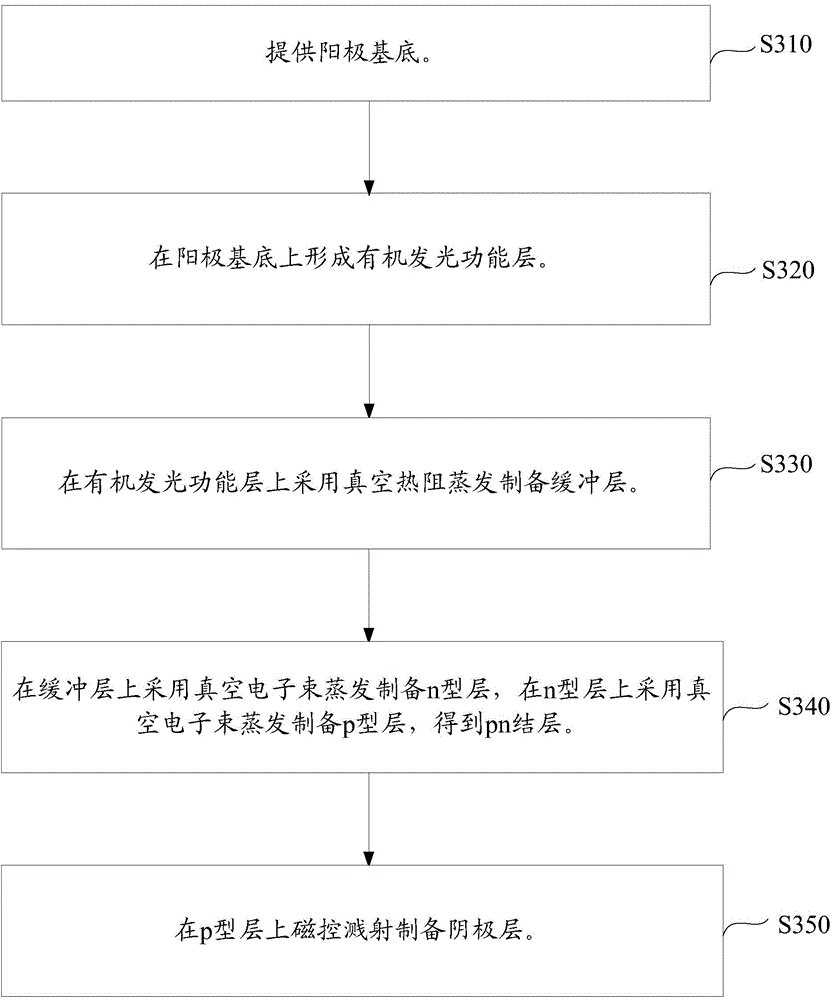
[0051] Such as image 3 As shown, a method for preparing an organic electroluminescent device in one embodiment includes the following steps:

[0052] Step S310: providing an anode substrate. Wherein, the anode substrate is transparent conductive glass. The transparent conductive glass may be indium tin oxide conductive glass (ITO), aluminum zinc oxide conductive glass (AZO) or indium zinc oxide conductive glass (IZO); preferably indium tin oxide glass (ITO); and indium tin oxide The sheet resistance of the conductive glass is 5Ω / □~100Ω / □.

[0053] Step S320: forming an organic light-emitting functional layer on the anode substrate.

[0054] Among them, the steps of forming the organic light-emitting functional layer on the anode substrate are: preparing a hole transport layer by vacuum evaporation on the anode substrate, preparing a light-emitting layer by vacuum thermal resistance evaporation on the hole transport layer, and using vacuum thermal evaporation on the light-e...

Embodiment 1

[0071] The structure of the organic electroluminescent device of the present embodiment is: ITO / NPB / NPB:Ir(MDQ) 2 (acac) / Bphen / LiF / ZnO / CuO / ITO.

[0072] The preparation of the organic electroluminescence device of this embodiment is as follows:

[0073] (1) Provide an ITO anode substrate and clean it, wherein the square resistance of the ITO anode substrate is 5Ω / □, and the ITO anode substrate is expressed as: ITO.

[0074] (2) Form an organic light-emitting functional layer on the anode substrate: in a vacuum of 1×10 -5 In the vacuum coating system of Pa, the hole transport layer is prepared by vacuum evaporation on the anode substrate, the thickness of the hole transport layer is 20nm, and the material is N,N'-diphenyl-N,N'-bis(1-naphthalene base)-1,1'-biphenyl-4,4'-diamine (NPB), the evaporation rate is 0.1nm / s, and the hole transport layer is expressed as: NPB;

[0075] In a vacuum of 1×10 -5 In the vacuum coating system of Pa, the light-emitting layer is prepared on t...

Embodiment 2

[0087] The structure of the organic electroluminescence device of the present embodiment is: ITO / MeO-TPD / Alq 3 :DCJTB / TPBi / CsF / SnO 2 / NiO / AZO.

[0088] The preparation of the organic electroluminescence device of this embodiment is as follows:

[0089] (1) Provide an ITO anode substrate and clean it. The sheet resistance of the ITO anode substrate is 100Ω / □, and the ITO anode substrate is expressed as: ITO.

[0090] (2) Form an organic light-emitting functional layer on the anode substrate: in a vacuum of 1×10 -3 In the vacuum coating system of Pa, the hole transport layer is prepared by vacuum evaporation on the anode substrate. The thickness of the hole transport layer is 60nm, and the material is (N,N,N',N'-tetramethoxyphenyl)- For p-diaminobiphenyl (MeO-TPD), the evaporation rate is 1nm / s, and the hole transport layer is expressed as: MeO-TPD;

[0091] In a vacuum of 1×10 -3 In the vacuum coating system of Pa, the light-emitting layer was prepared on the hole transpor...


PUM


Abstract

An organic electroluminescent device comprises an anode substrate, an organic light-emitting functional layer, a buffer layer, a pn node layer and a cathode layer which are sequentially laminated, wherein the pn node layer comprises an n-type layer laminated on the buffer layer and a p-type layer laminated on the n-type layer; the cathode layer is laminated on the p-type layer; the anode substrate is made of transparent conductive glass; the buffer layer is made of lithium fluoride, cesium fluoride or sodium fluoride; the n-type layer is made of zinc oxide, tin oxide or cerium dioxide; the p-type layer is made of nickel oxide or copper oxide; the cathode layer is made of an indium tin oxide conductive thin film, an aluminum zinc oxide conductive thin film or an indium zinc oxide conductive thin film. The organic electroluminescent device has relatively high luminous performance and is uniform in luminescence. The invention further provides a manufacturing method of the organic electroluminescent device.

Description

technical field [0001] The invention relates to the field of manufacturing organic electroluminescent devices, in particular to an organic electroluminescent device and a preparation method thereof. Background technique [0002] Organic Light Emission Diode, hereinafter referred to as OLED, has the characteristics of high brightness, wide range of material selection, low driving voltage, fully cured active light emission, etc., and has the advantages of high definition, wide viewing angle, and fast response speed. It is a display technology and light source with great potential, which conforms to the development trend of mobile communication and information display in the information age, as well as the requirements of green lighting technology, and is the focus of many researchers at home and abroad. [0003] Among the currently used OLED light emitting devices, the double-sided OLED has great application advantages, which can realize omni-directional 360-degree lighting or...

Claims


Application Information

Patent Timeline
Patent Type & Authority Applications(China)
IPC IPC(8): H01L51/50H01L51/52H01L51/54H01L51/56
CPCH10K30/865H10K50/80H10K2102/00H10K2102/302H10K71/00
Inventor 周明杰冯小明钟铁涛王平
Owner OCEANS KING LIGHTING SCI&TECH CO LTD
Why Eureka
Try Eureka