Manufacturing method of micro lens
A manufacturing method and technology of microlens, applied in the direction of lens, photoplate-making process of patterned surface, optics, etc., can solve the problems of poor process repeatability, achieve the effect of improving process repeatability, easy realization, and increased utilization rate
- Summary
- Abstract
- Description
- Claims
- Application Information
AI Technical Summary
Problems solved by technology
Method used
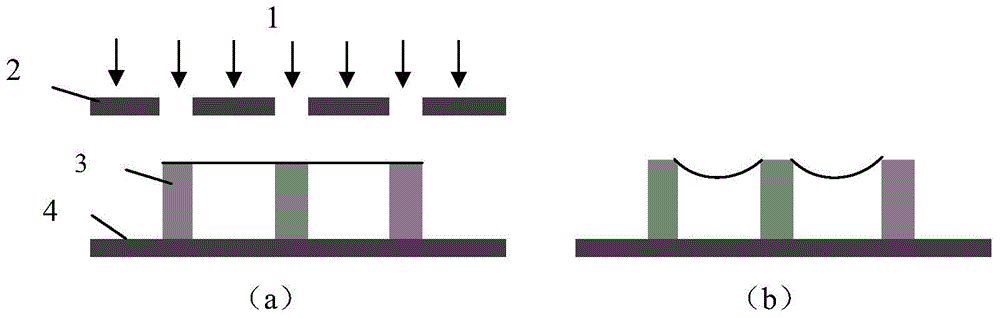
Image

Examples
example 1
[0027] Example 1, Fabrication of Concave Cylindrical Mirror Array
[0028] The planar structure of the concave cylindrical mirror array is a grating structure, and the effective control of the morphology of the microlens can be realized through the selection of the grating structure parameters, the selection of the photoresist and the selection of the corresponding process conditions. Taking the array period as 110 microns as an example, SU8 negative photoresist is selected to fabricate the concave cylindrical mirror array.
[0029] The dimensions of the planar structure are first given: a grating structure with a period of 110 μm, a duty ratio of 1:10, and a line length of 1 cm.
[0030] The specific production is as follows:
[0031] 1) Process the corresponding optical mask according to the dimensions given above;
[0032] 2) Clean the glass substrate, spin-coat SU8 photoresist, bake on a hot table at 96 degrees for 30 minutes, and obtain a SU8 photoresist layer with a th...
example 2
[0037] Example 2, the production of concave honeycomb lens array
[0038] The planar structure of the concave honeycomb lens array is a honeycomb structure, and the microlens morphology can be effectively controlled by selecting the parameters of the honeycomb structure, the photoresist and the corresponding process conditions. Taking an array period of 155 microns as an example, KMPR negative photoresist is selected to make a concave honeycomb lens array.
[0039] Firstly, the size of the planar structure is given: a honeycomb structure with a period of 155 microns. In order to improve the utilization rate of the light source by the lens array, the side width of the honeycomb structure is 5 microns.
[0040] The specific production is as follows:
[0041] 1) Process the corresponding optical mask according to the dimensions given above;
[0042] 2) Clean the glass substrate, spin-coat KMPR photoresist, bake on a hot table at 100 degrees for 15 minutes, and obtain a KMPR pho...
PUM
 Abstract
Description
Claims
Application Information