Method and device for realizing low-cost tunable semiconductor laser based on reconstruction-equivalent chirp and series/parallel hybrid integration technologies

An equivalent chirp and laser technology, applied in the field of optoelectronics, can solve the problems of increasing laser cost, reducing laser performance, and high cost

Inactive Publication Date: 2015-05-20
NANJING UNIV SCI PARK DEV
View PDF5 Cites 11 Cited by
  • Summary
  • Abstract
  • Description
  • Claims
  • Application Information

AI Technical Summary

Problems solved by technology

However, due to the high cost of the electron beam exposure technology, the writing speed is very slow, and due to the characteristics of the electron beam itself, the accuracy of the working

Method used


Image

  • Method and device for realizing low-cost tunable semiconductor laser based on reconstruction-equivalent chirp and series/parallel hybrid integration technologies
  • Method and device for realizing low-cost tunable semiconductor laser based on reconstruction-equivalent chirp and series/parallel hybrid integration technologies
  • Method and device for realizing low-cost tunable semiconductor laser based on reconstruction-equivalent chirp and series/parallel hybrid integration technologies

Examples


example 1

[0028] [Example 1] 3X4 segment tunable semiconductor laser based on series / parallel hybrid integration:

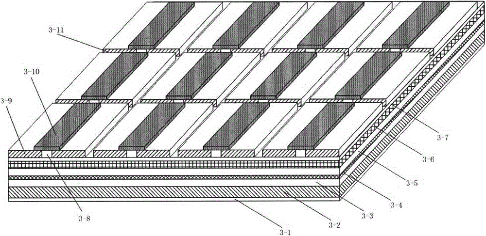
[0029] Such as figure 1 As shown, the epitaxial material of the device is described as follows: First, an N-type InP buffer layer (thickness 200nm, doping concentration of about 1.1X10 18 cm -2 ), 100nm thick amorphous doped lattice matching InGaAsP waveguide layer, strained InGaAsP multi-quantum well layer (optical fluorescence wavelength 1.52 microns, 7 quantum wells: well width 8nm, 0.5% compressive strain; barrier width 10nm, lattice matching material ), 70nm thick InGaAsP grating material layer. Then, a mask plate containing the sampling period distribution required by the equivalent grating is fabricated using common microelectronics technology. Next, the grating structure is produced by sampling mask and holographic interference exposure, and then the second epitaxial 100nm thick P-type lattice matching InGaAsP waveguide layer (the doping concentration is about 1...

example 2

[0033] [Example 2] Multi-segment tunable semiconductor laser based on series / parallel hybrid integration:

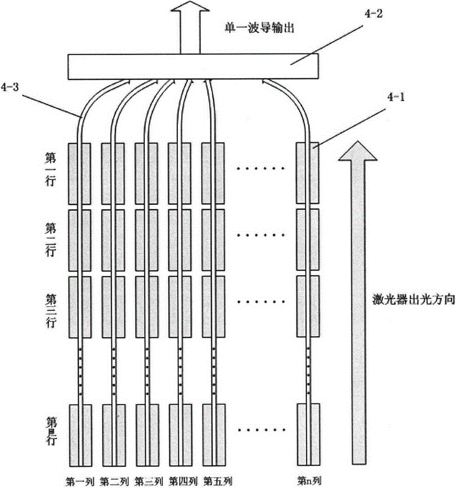
[0034] Such as figure 2 As shown, the 3X4 segment tunable laser in Example 1 can be extended to an mxn segment tunable laser including m rows and n columns of lasers, and the material structure is the same as that of Example 1, wherein there are all between rows and columns and between columns and columns Make a 75um electrical isolation slot. In the process of making electrical isolation, the ohmic contact layer InGaAsP in the corresponding area of ​​the laser is first etched away by dry or wet methods, and then ion implantation is performed in this area, and then the insulating material SiO2 with a thickness of 300nm is covered. The SiO over the ridge waveguide is then 2 The material is etched away and the P-type electrode on the front of the laser is made. The N-type electrode on the back is fabricated after the laser substrate is thinned. There are anti-reflecti...


PUM


Abstract

A method and a device for realizing a low-cost tunable semiconductor laser based on a reconstruction-equivalent chirp technology belong to the technical field of optoelectronics, and relate to the design and manufacture of a complex distributed feedback tunable semiconductor laser. The invention aims to provide a low-cost tunable distributed feedback semiconductor laser for the future WDM-PON market by adopting the reconstruction-equivalent chirp technology for low-cost manufacture. The basic technology is that a plurality of distributed feedback semiconductor lasers of different wavelengths are integrated on the same chip through a series/parallel hybrid mode, and a mode of crosstalk isolation between adjacent laser chips is provided. According to the invention, DFB lasers of different working wavelengths based on the reconstruction-equivalent chirp technology are integrated by a series/parallel combination mode, one of the lasers is selected by current to work, and the working wavelength of the laser can be controlled by adjusting the temperature or current, thus realizing continuous tuning of the working wavelength of the laser.

Description

technical field [0001] The invention belongs to the field of optoelectronic technology, and is related to distributed feedback semiconductor lasers, in particular to the design and manufacture of complex distributed feedback tunable semiconductor lasers, more specifically, a low-cost tunable distributed feedback based on reconstruction-equivalent chirp technology Method and apparatus for semiconductor lasers. Background technique [0002] In the past 20 years, the continuous growth of the global broadband demand has greatly promoted the development of the optical fiber communication industry, and people have put forward a variety of ideas and solutions that can increase the communication capacity, among which Dense Wavelength Division Multiplexing (DWDM) is a Efficient and flexible, and easy to upgrade and transform on the basis of existing equipment, it has won people's favor and has been applied on a large scale. DWDM technology improves system transmission capacity by in...

Claims


Application Information

Patent Timeline
IPC IPC(8): H01S5/06H01S5/40
Inventor 李连艳唐松陈向飞张云山陆骏
Owner NANJING UNIV SCI PARK DEV
Why Eureka
Try Eureka