Organic electroluminescence device and preparation method thereof
An electroluminescent device and luminescent technology, which is applied in the direction of electric solid-state devices, semiconductor/solid-state device manufacturing, electrical components, etc., can solve the problems of total reflection loss, low light extraction performance, poor refractive index, etc., and achieve the reduction of attenuation speed, Improve luminous efficiency and stabilize luminous color
- Summary
- Abstract
- Description
- Claims
- Application Information
AI Technical Summary
Problems solved by technology
Method used
Image
Examples
preparation example Construction
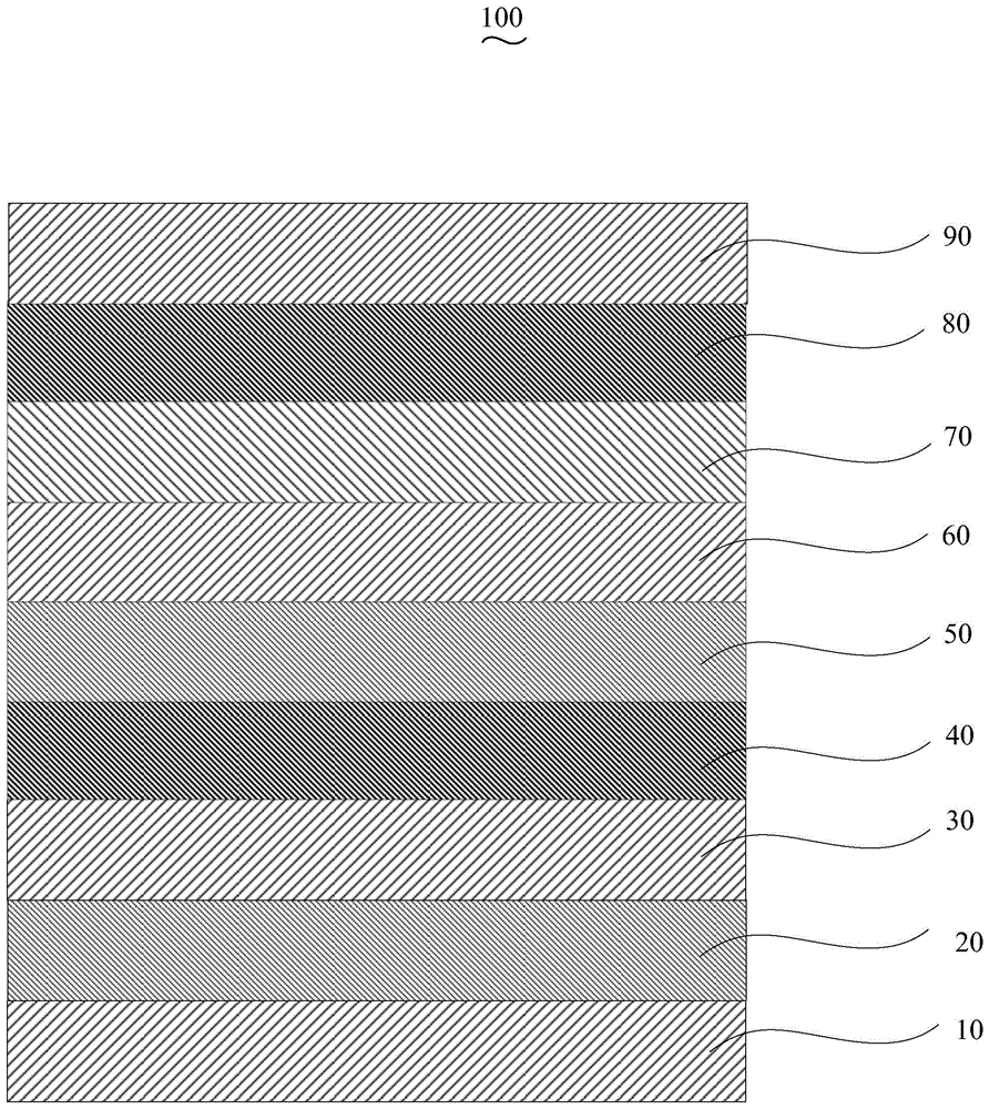
[0037] The preparation method of the organic electroluminescence device 100 of an embodiment, it comprises the following steps:
[0038] Step S110 , preparing the scattering layer 20 on the surface of the glass substrate 10 by electron beam evaporation.
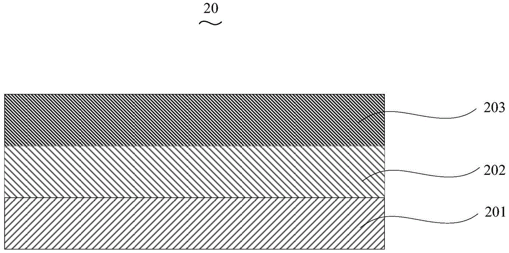
[0039] The scattering layer 20 is formed on one side surface of the glass substrate 10 . The scattering layer 20 is composed of a first luminescent material layer 201 , a metal oxide doped layer 202 and a second luminescent material layer 203 . The first luminescent material layer 201 is prepared on the surface of the glass substrate 10 by thermal resistance evaporation, and the metal oxide doped layer 202 is prepared on the surface of the first luminescent material layer 201 by electron beam evaporation. The metal oxide The material-doped layer 202 includes a first metal oxide and the second metal oxide doped in the first metal oxide, and the HOMO energy level of the first metal oxide is -5.2eV~-6.0 eV, the refractive inde...
Embodiment 1
[0059] The structure prepared in this example is glass substrate / Alq 3 / MoO 3 :ZrO 2 / Alq 3 / ITO / MoO 3 / NPB / Alq 3 / TAZ / CsF / Ag organic electroluminescent device, in this embodiment and the following embodiments, " / " indicates a layer, and ":" indicates doping.
[0060] The glass substrate is N-LASF44. After rinsing the glass substrate with distilled water and ethanol, soak it in isopropanol for one night. A scattering layer is prepared on a glass substrate. The scattering layer is composed of a first luminescent material layer, a metal oxide doped layer and a second luminescent material layer. The first luminescent material layer is prepared by thermal resistance evaporation on the surface of a glass substrate, and the material is Alq 3 , with a thickness of 45nm, a metal oxide doped layer was prepared on the surface of the first luminescent material layer by electron beam evaporation, and the material was MoO 3 :ZrO 2 , MoO 3 with ZrO 2 The mass ratio is 12:1, the thi...
Embodiment 2
[0068] The structure prepared in this example is glass substrate / DCJTB / WO 3 :MgO / ADN / IZO / MoO 3 / TCTA / ADN / Bphen / CsN 3 / Al organic electroluminescent devices.
[0069] The glass substrate is N-LAF36. After rinsing the glass substrate with distilled water and ethanol, soak it in isopropanol for one night to prepare a scattering layer on the glass substrate. The scattering layer consists of the first luminescent material layer, the metal oxide doped layer Composed with the second luminescent material layer, the first luminescent material layer is prepared by thermal resistance evaporation on the surface of the glass substrate. Layer, material is WO 3 : MgO, WO 3 The mass ratio to MgO is 10:1, the thickness is 300nm, and the second luminescent material layer is prepared by thermal resistance evaporation on the surface of the metal oxide doped layer, the material is ADN, and the thickness is 2nm. Then IZO is prepared on the scattering layer with a thickness of 80nm, which is pr...
PUM
 Abstract
Description
Claims
Application Information


