Manufacturing method of flexible buried electrode film using thermal lamination transfer

A flexible electrode and thin film technology, which is applied in the direction of thermoplastic polymer dielectric, printed circuit manufacturing, cable/conductor manufacturing, etc., can solve the problems of conductive thin film, wet dissolution speed reduction, etc., to prevent pattern damage or short circuit, excellent resistance value , Eliminate the effect of plane difference

Inactive Publication Date: 2015-05-27
LG CHEM LTD
View PDF8 Cites 15 Cited by
  • Summary
  • Abstract
  • Description
  • Claims
  • Application Information

AI Technical Summary

Problems solved by technology

However, this technique is problematic due to the complex process of externally coating and curing the curable polymer and wet stripping
Moreover, during the wet stripping of the sacrificial layer, the exposed area of ​​the sacrificial layer is very small in the lateral direction of the film, so that the wet dissolution rate will be reduced, making it worse to expand the large-area conductive film

Method used


Image

  • Manufacturing method of flexible buried electrode film using thermal lamination transfer
  • Manufacturing method of flexible buried electrode film using thermal lamination transfer
  • Manufacturing method of flexible buried electrode film using thermal lamination transfer

Examples


example 1

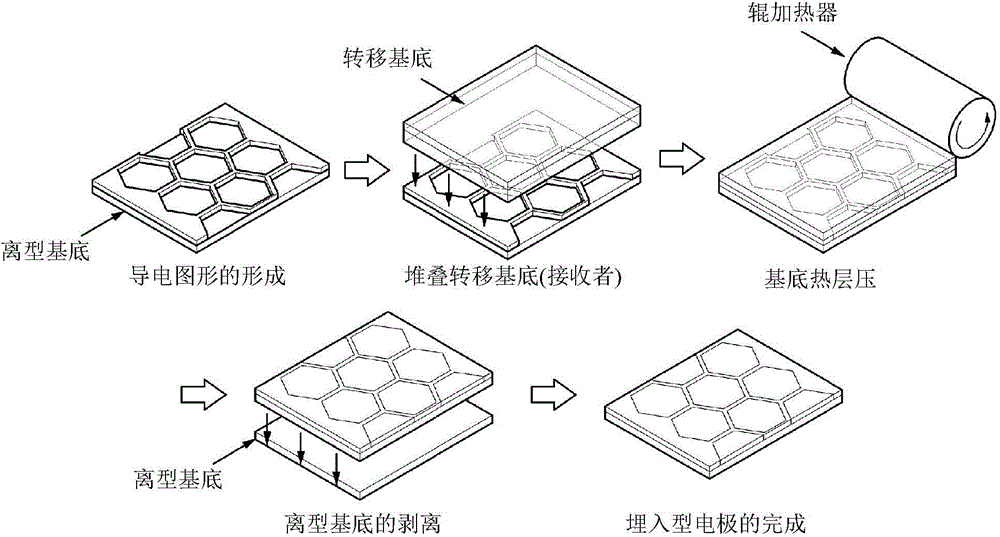
[0102] A PET substrate with a thickness of 180 μm was coated with a 5 mm thick polydimethylsiloxane (PDMS) (SYLGARD 184, purchased from Dow Corning Corp.) solution (mixing ratio 1:9), and then cured at 70 °C for 6 hours to prepare a release substrate. Using e-electron beam deposition machine (base pressure: 8×10 -7 Torr, working pressure: 5×10 -5 trust, ) A 150 nm thick Al foil was deposited on the release surface of the release substrate.

[0103] Using AZ1518 photoresist, coating, drying, mask exposure and development were performed to form a pattern on the Al deposition film.

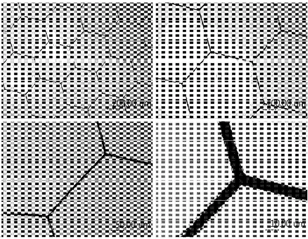
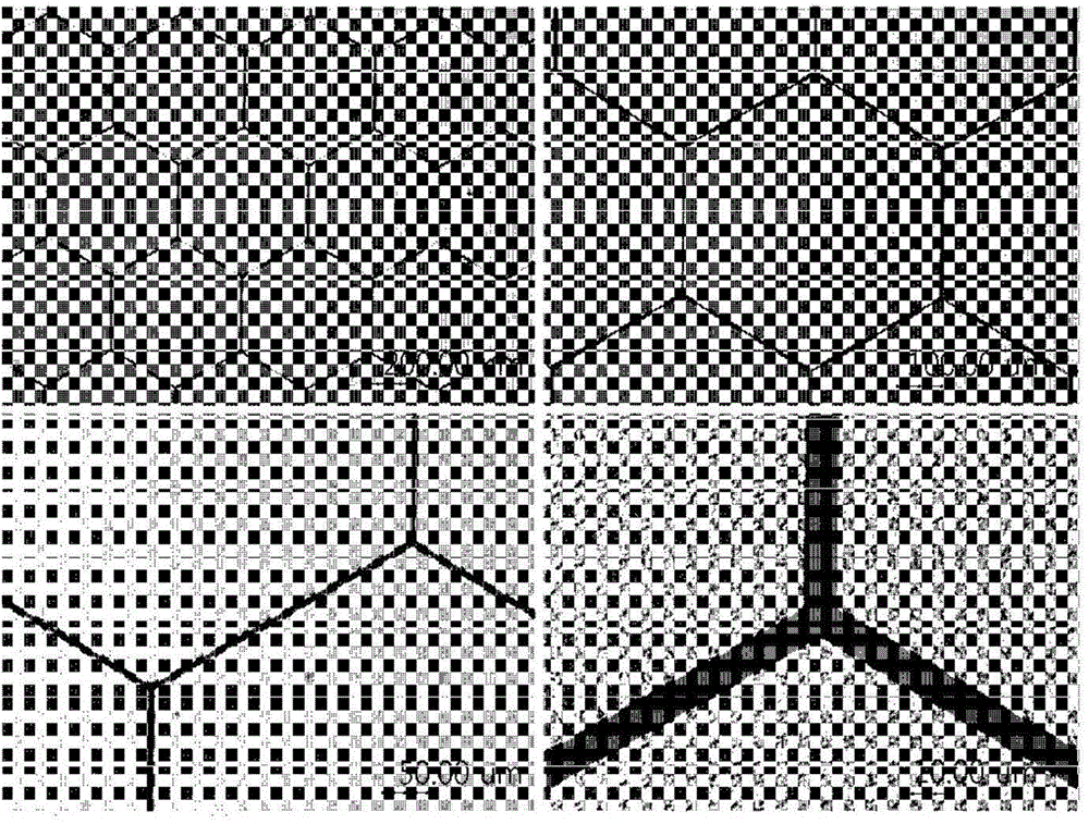
[0104] The formed photoresist pattern is subjected to wet etching (phosphoric acid-based Al etching solution) or dry etching (ICP-RIE) to form an Al electrode pattern. Based on observations through an optical microscope, such as figure 2 Al electrode patterns are formed as shown.

[0105] On the Al electrode pattern, place a 250 μm EVA (ethylene vinyl acetate) film (pouch laminating film, pur...

example 2

[0108] Fabricate the flexible conductive embedded electrode film in the same manner as in Example 1, the difference is that, with 1~5wt% dilute fluorinated silane (OPTOOL TM , purchased from Daikin Industries, LTD.) solution was spin-coated on a PET substrate with a thickness of 180 μm, and then dried at 120° C. for 30 minutes to prepare a release substrate.


PUM

PropertyMeasurementUnit
thicknessaaaaaaaaaa
thicknessaaaaaaaaaa
widthaaaaaaaaaa

Abstract

The present invention relates to a method for manufacturing a flexible buried electrode film and a flexible buried electrode film manufactured by the same. The method includes the steps of: 1) preparing a release base material; 2) forming a conductive pattern layer on the release base material; 3) locating a transfer base material on the conductive pattern layer and then inserting into or burying in the surface of the transfer base material the conductive pattern layer formed on the release base material by thermal and pressure fusion; and 4) separating the release base material from the conductive pattern layer.

Description

technical field [0001] The invention relates to a method for manufacturing an embedded flexible electrode film by using thermal lamination transfer. Background technique [0002] With recent advancements in the electrical and electronic industries, various home appliances and electronic products have been developed. Due to the trend toward more compact electronic products, intense research is continuing to meet the technical demands of reducing the size and thickness of such electronic products. [0003] A circuit board includes circuit wires for electrically connecting electronic devices, electronic devices, and semiconductor packages. Although a conventional circuit board is composed of metal wiring patterns formed on an insulating board, when the circuit wires on the insulating board cross on the same plane, a short circuit may occur between the circuit wires. Accordingly, circuit boards typically include multiple layers of circuit patterns that are electrically insulat...

Claims


Application Information

Patent Timeline
Patent Type & Authority Applications(China)
IPC IPC(8): H01B13/00H01B5/14
CPCH05K3/207H05K2201/0129H05K2201/0376H05K2201/09681H05K2203/1545H05K2203/06H01B5/00H01B5/102H01B5/14H01B5/16H01B13/00H01B17/62H01L31/022425H01L31/022466
Inventor 朴正岵辛富建金在镇李钟炳郑镇美
Owner LG CHEM LTD
Why Eureka
Try Eureka