Optical waveguide devices

一种器件、脊部的技术,应用在光波导器件领域,能够解决传播损失变大、难加工台横向移动等问题,达到抑制传播损失的效果

Active Publication Date: 2015-06-03
NGK INSULATORS LTD
View PDF8 Cites 7 Cited by
  • Summary
  • Abstract
  • Description
  • Claims
  • Application Information

AI Technical Summary

Problems solved by technology

However, during machining and laser ablation, it is difficult to move the processing table laterally to the direction of travel
In addition, even if the processing table is moved laterally, unlike straight processing, the cross-sectional shape of the ridges and grooves will be distorted, so the propagation loss will increase

Method used


Image

  • Optical waveguide devices
  • Optical waveguide devices
  • Optical waveguide devices

Examples


Embodiment 1

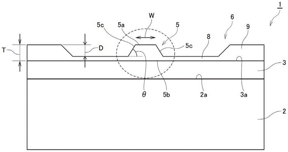
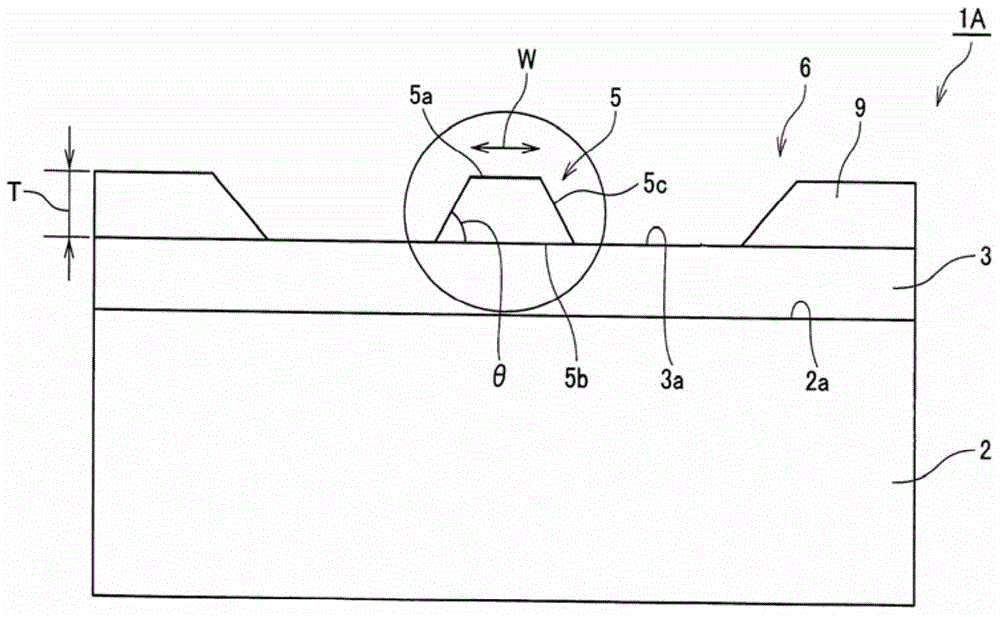
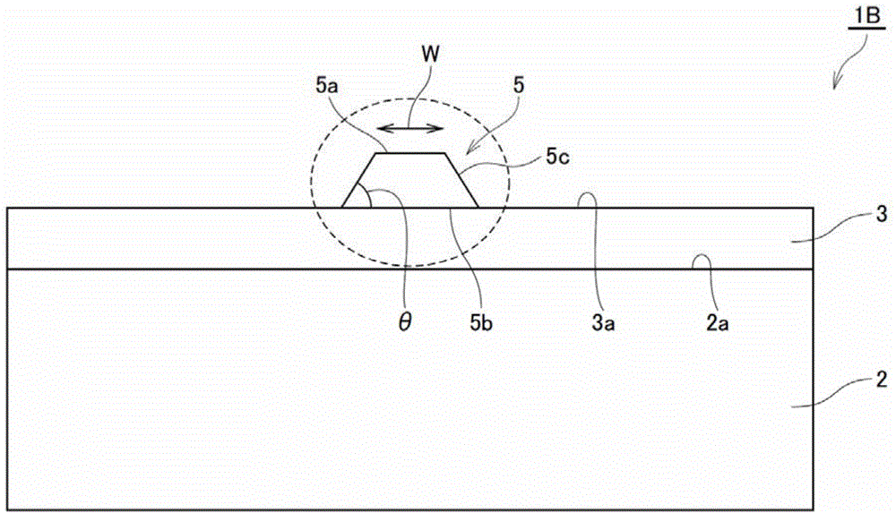
[0078] make figure 1 , Figure 4 (a) and Figure 5 Documented device 1.

[0079] Specifically, a dielectric layer 3 (thickness 2.0 μm) / SiO made of lithium niobate doped with MgO 2 A laminated body of the support substrate 2 with a thickness of .5 mm consisting of the clad layer / adhesive layer / Y plate not doped with lithium niobate. On this dielectric layer 3, Ta 2 o 5 membrane.

[0080] Next, a molybdenum film having a thickness of 100 nm was formed on the upper surface 3 a of the dielectric layer 3 and the bottom surface of the support substrate 2 . Next, a resist pattern is formed on the dielectric layer and the molybdenum film by photolithography (resist coating and development). In addition, a resist is applied to the entire bottom surface of the support substrate 2 . Next, the molybdenum film was wet-etched to remove the resist, and a pattern made of the molybdenum film was formed.

[0081] Next, the laminated body was dipped in 50% HF whose temperature was adjus...

Embodiment 2

[0098] A device was produced in the same manner as in Example 1. However, the material of the dielectric layer 3 is a lithium tantalate single crystal doped with MgO. As a result, the same result as in Example 1 was obtained. In addition, as a result of the tape test, it was confirmed that no film was attached to the tape and no ridges were peeled off from the device.

Embodiment 3

[0100] A device was produced in the same manner as in Example 1. However, the material of the dielectric layer 3 is yttrium vanadate crystal. In order to confirm the performance of the optical waveguide, the propagation loss at a wavelength of 980 nm was measured in the same manner as in Example 1, and the result was 0.5 dB / cm. In addition, as a result of the tape test, it was confirmed that no film was attached to the tape and no ridges were peeled off from the device.


PUM

PropertyMeasurementUnit
etching rateaaaaaaaaaa

Abstract

An optical waveguide device 1 includes a thin layer 3 and a ridge portion 5 loaded on the thin layer 3. The thin layer 3 is made of an optical material selected from the group consisting of lithium niobate, lithium tantalate, lithium niobate-lithium tantalate, yttrium aluminum garnet, yttrium vanadate, gadolinium vanadate, potassium gadolinium tungstate; and potassium yttrium tungstate. The ridge portion 5 is made of tantalum pentoxide and has a trapezoid shape viewed in a cross section perpendicular to a direction of propagation of light. The ridge portion is not peeled off from the thin layer in a tape peeling test.

Description

technical field [0001] The present invention relates to optical waveguide devices. Background technique [0002] Nonlinear optical crystals such as lithium niobate or lithium tantalate single crystals have large second-order nonlinear optical coefficients, and quasi-phase-matched (Quasi-Phase-Matched: QPM) can be realized by forming a periodic polarization inversion structure in these crystals. ) mode of second harmonic generation (Second-Harmonic-Generation: SHG) equipment. Furthermore, by forming a waveguide within this periodic polarization inversion structure, a high-efficiency SHG device can be realized, which can be widely used in optical communication, medicine, photochemistry, various optical measurements, and the like. [0003] Generally, SHG equipment must have a fundamental wave light source called excitation light from the outside. For example, in the case of a green SHG laser, the fundamental wave light source sometimes uses a semiconductor laser in the 800nm ​...

Claims


Application Information

Patent Timeline
Patent Type & Authority Applications(China)
IPC IPC(8): G02B6/125
CPCG02B6/122G02B6/125G02B1/10G02B2006/12176G02F1/3503G02F1/3501
Inventor 浅井圭一郎山口省一郎
Owner NGK INSULATORS LTD
Why Eureka
Try Eureka