Manufacturing method of MEMS chip insensitive to packaging stress and MEMS chip

A technology of packaging stress and manufacturing method, which is applied in the field of MEMS chips, can solve the problems that the contact area affects the ability of MEMS devices to resist mechanical impact, the soft glue cannot withstand too high temperature, and the MEMS devices cannot work, etc., so as to simplify the wafer processing process , Reduce material cost, low cost effect

Active Publication Date: 2015-06-10
ANHUI BEIFANG XINDONG LIANKE MICROSYST TECH
View PDF6 Cites 18 Cited by
  • Summary
  • Abstract
  • Description
  • Claims
  • Application Information

AI Technical Summary

Problems solved by technology

But the disadvantages of these methods are: first, the material with the same thermal expansion coefficient as the Si material cannot be used to make the tube shell; two, the soft die-mounting adhesive will cause some MEMS devices to fail to work, because the tube shell needs to be provided for the active MEMS structure. Reaction force, and the soft rubber can not withstand too high temperature, and is not compatible with some packaging processes, such as metal fusion sealing; Third, the contact area between the MEMS chip and the package shell is too small, which will affect the

Method used


Image

  • Manufacturing method of MEMS chip insensitive to packaging stress and MEMS chip
  • Manufacturing method of MEMS chip insensitive to packaging stress and MEMS chip
  • Manufacturing method of MEMS chip insensitive to packaging stress and MEMS chip

Examples


Example Embodiment

[0042] The preferred embodiments of the present invention will be described in detail below with reference to the accompanying drawings, so that the advantages and features of the present invention can be more easily understood by those skilled in the art, and the protection scope of the present invention can be more clearly defined.

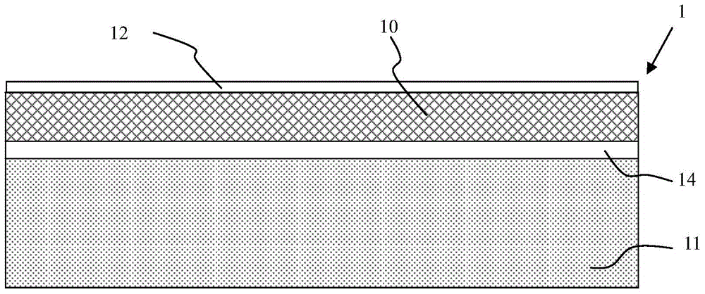
[0043] see figure 1 , the material of the top layer Si 10 of the SOI wafer 1 is heavily doped monocrystalline silicon with a crystal orientation, and a first oxide layer 12 is grown on the top layer Si 10 by general semiconductor processing technology, and its material is silicon dioxide , formed by thermal oxidation, the thickness of the top layer Si 10 is determined according to the thickness of the lower electrode of the MEMS chip, generally 5-60 microns; the material of the bottom layer Si 11 of the SOI wafer 1 is also a heavily doped monolayer with a crystal orientation. Crystalline silicon, its thickness is generally 300-800 microns; the...


PUM


Abstract

The invention discloses a manufacturing method of an MEMS chip insensitive to packaging stress. The manufacturing method comprises the steps of firstly, taking an SOI wafer, forming a lower electrode by use of top-layer Si and etching the top-layer Si to form lower electrode patterns, secondly, taking a single crystal Si wafer and performing photoetching and Si etching to form a substrate wafer, thirdly, aligning the SOI wafer to the substrate wafer, performing silicon-silicon dioxide bonding and annealing to form a bonded wafer, and grinding the bottom-layer Si of the SOI wafer in the bonded wafer to form an MEMS activity structure layer, fourthly, depositing a metal layer on the MEMS activity structure layer to form a metal pad, fifthly, etching the MEMS activity structure layer and releasing the MEMS activity structure layer, sixthly, taking a single-crystal Si wafer, and performing photoetching and Si etching to form a cover plate wafer, seventhly, aligning and bonding the cover plate wafer to the bonded wafer and annealing to form a sealed wafer, and finally cutting the cover plate wafer and the sealed wafer to obtain the MEMS chip. The manufacturing method is short in process and high in rate of finished products; the manufactured MEMS chip is insensitive to the packaging stress.

Description

technical field [0001] The invention relates to the technical field of MEMS wafer manufacturing, in particular to a method for manufacturing a MEMS chip that is not sensitive to packaging stress and the manufactured MEMS chip. Background technique [0002] MEMS (Micro-Electro-Mechanical Systems) is the abbreviation of micro-electro-mechanical systems. MEMS chip manufacturing technology uses micro-fabrication technology, especially semiconductor wafer manufacturing technology, to manufacture various micro-mechanical structures, combined with application-specific control integrated circuits (ASICs), Composition of intelligent micro-sensors, micro-actuators, micro-optical devices and other MEMS components. MEMS components have the advantages of small size, low cost, high reliability, strong resistance to harsh environments, low power consumption, high intelligence, easy calibration, and easy integration. They are widely used in consumer electronics products, such as mobile phon...

Claims


Application Information

Patent Timeline
IPC IPC(8): B81C1/00B81B7/02
Inventor 华亚平
Owner ANHUI BEIFANG XINDONG LIANKE MICROSYST TECH
Why Eureka
Try Eureka