

Alkaline-developable photosensitive solder resist ink for FPC, preparation method, application and product
A technology of photosensitive solder resist ink and alkali development, applied in ink, optical mechanical equipment, applications, etc., can solve the problems of being unable to adapt to FPC applications, not having too many requirements for flexibility, and poor folding resistance, so as to achieve good adhesion to substrates , good flexibility, short dry time
- Summary
- Abstract
- Description
- Claims
- Application Information
AI Technical Summary
Problems solved by technology
Method used
Image

Examples
example 1
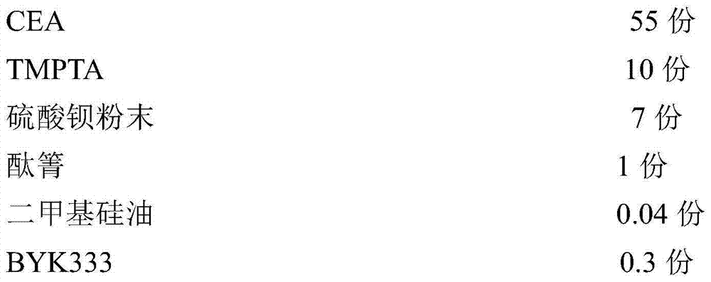
[0052] The formula is as follows:
[0053] Component A:
[0054]
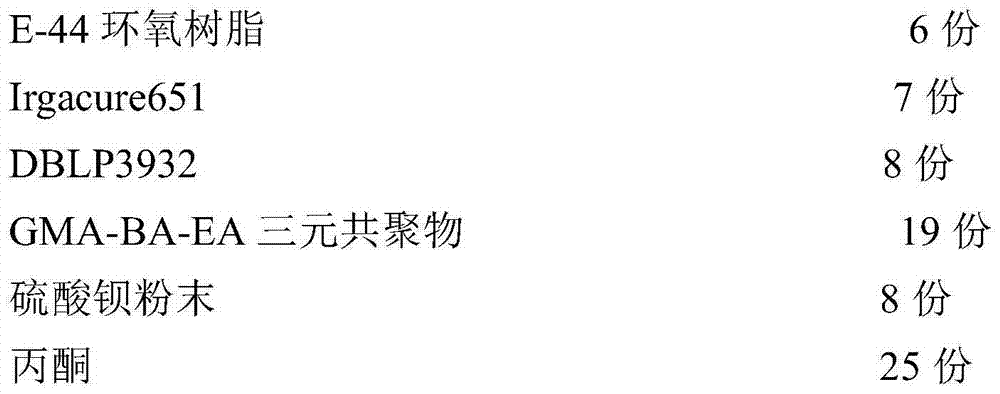
[0055] Component B:
[0056]
[0057] The preparation steps are as follows:
[0058] According to the above formula, add the various materials in component A into the batching container, stir and mix well, then send it to the three-roller mill for dispersion and grinding for two to three times until the fineness is ≤10μm to obtain the component A of the solder resist ink ; The same method to obtain the B component of the solder resist ink. Store airtight at low temperature. Before use, mix the two components A and B in a ratio of 1:1 before use.
[0059] The film forming method is as follows:
[0060] Screen print the above ink on the FPC, pre-bake it at 85°C for 25min, then expose it to light for 60s with UV (wavelength λ=365nm, irradiation distance 20cm) for curing, develop it with 2% sodium carbonate aqueous solution, and then heat it at 140°C After curing for 30 minutes, a dense and smooth ink f...
example 2
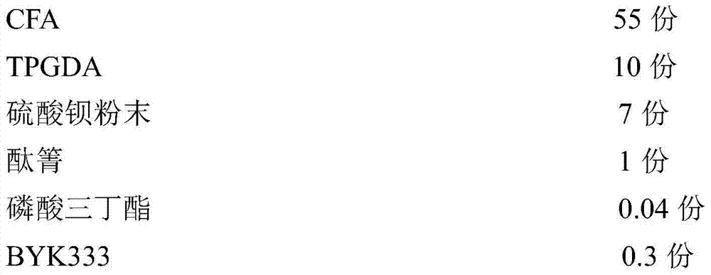
[0070] The formula is as follows:
[0071] Component A:
[0072]
[0073] Component B:
[0074]
[0075] The preparation and film-forming methods are the same as in Example 1, and the test results are shown in Table 1.
example 3
[0077] The formula is as follows:
[0078] Component A:
[0079]
[0080]
[0081] Component B:
[0082]
[0083] The preparation and film-forming methods are the same as in Example 1, and the test results are shown in Table 1 below.
[0084] Table 1 Example 1-Example 3 test results
[0085]
[0086] It can be seen from Table 1 that the solder resist inks obtained in the above three examples all have good process performance: the surface dry time is short (not more than 25min at 85°C), and the development is clear and fast (not more than 2min in 2% Na2CO3 aqueous solution) , thereby greatly improving production efficiency; the cured coating film has the advantages of high hardness (pencil hardness ≥ 4H), good adhesion to the substrate (adhesion level), good chemical resistance and bending resistance, etc., and can meet the requirements of micro Performance requirements of solder resist ink for circuit FPC.
[0087] In addition, reduce the amount of the alkali-s...
PUM
 Abstract
Description
Claims
Application Information