Supercharge Your Innovation With Domain-Expert AI Agents!

Reflection element with inner surface provided with micro-convex structure array and manufacturing method of reflection element

A manufacturing method and micro-convex structure technology, applied in optical components, optics, instruments, etc., can solve the problems of high cost, inability to realize precision manufacturing of large-area surface microstructures, and difficult processing, etc., and achieve simple manufacturing process and microstructure The effect of high reproduction ratio and precise size

Inactive Publication Date: 2015-07-01
SOUTH CHINA UNIV OF TECH
View PDF3 Cites 3 Cited by
  • Summary
  • Abstract
  • Description
  • Claims
  • Application Information

AI Technical Summary

Problems solved by technology

However, most of these manufacturing methods cannot realize the precise manufacturing of large-area surface microstructures due to the disadvantages of difficult processing and high cost.
It is a great challenge to fabricate large-area ordered microstructure arrays on the inner surface.

Method used


Image

  • Reflection element with inner surface provided with micro-convex structure array and manufacturing method of reflection element
  • Reflection element with inner surface provided with micro-convex structure array and manufacturing method of reflection element
  • Reflection element with inner surface provided with micro-convex structure array and manufacturing method of reflection element

Examples


Embodiment 1

[0062] A method for manufacturing a reflective element with an array of micro-convex structures on its inner surface, comprising the steps of:

[0063] S1 Preparation steps of flexible transfer film using letterpress hot embossing coating:

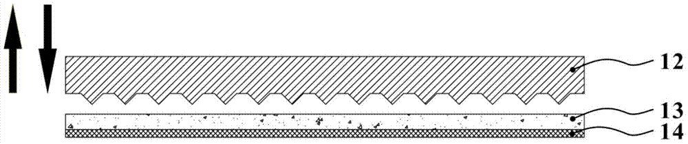
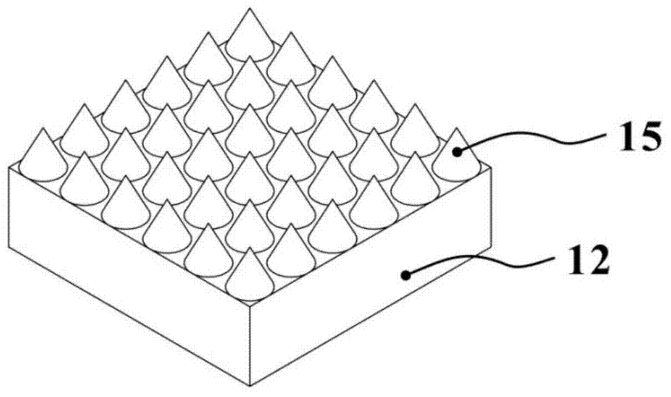
[0064] S1.1 Select polytetrafluoroethylene film substrate (PFTE) with a thickness of 30 μm. Using the scraper coating method, the silicone resin is coated on the polytetrafluoroethylene film base material, and Dow Corning OE-6550 silica gel is selected for use, and the coating thickness is 30 μm. is 2.5μm, the radius of the tip of the cone is 75nm, and the height of the cone is 3μm, such as figure 2 shown.

[0065] S1.2 Preheat the coated silica gel wet film from room temperature to 80°C at a heating rate of 20°C / min, and keep it at 80°C for 3.5min. Then the temperature was raised to 110°C, the heating rate was 30°C / min, and the temperature was kept at 110°C for 2 minutes. After step-by-step curing, the silicone wet film reaches a sem...

Embodiment 2

[0077] A method for manufacturing a reflective element having an array of micro-convex structures on its inner surface, comprising the following steps:

[0078] S1 Preparation steps of flexible transfer film with letterpress hot embossing coating

[0079] S1.1 Tetrafluoroethylene film substrate (PFTE), with a thickness of 30 μm. Polydimethylsiloxane (PDMS) was coated on the polytetrafluoroethylene film substrate by spin coating, and Dow Corning Sylgard 184 was selected, and the coating thickness was 50 μm.

[0080] S1.2 Preheat the coated PDMS wet film from room temperature to 45°C at a heating rate of 10°C / min, and keep it at 45°C for 20min. Then the temperature was raised to 60°C with a heating rate of 15°C / min, and the temperature was kept at 60°C for 15 minutes. After step-by-step curing, the silicone wet film reaches a semi-cured state as a whole.

[0081] S1.3 Pass the semi-cured PDMS coating at a constant speed of 100mm / s through an 80mm-long heating tunnel with a te...


PUM

PropertyMeasurementUnit
heightaaaaaaaaaa
diameteraaaaaaaaaa
heightaaaaaaaaaa

Abstract

The invention discloses a reflection element with an inner surface provided with a micro-convex structure array and a manufacturing method of the reflection element. The manufacturing method comprises the following steps: (S1) preparing a flexible transfer adhesive film of a letterpress thermal printing coating; (S2) modifying a curved surface of a male mold by virtue of seal-exhausting negative pressure adsorption; (S3) carrying out microinjection molding on a thermoplastic or thermoset sizing material; and (S4) carrying out mold release, ultrasonic cleaning and inner surface vacuum aluminizing. A micro-convex structure of the reflection element is a cone body or a table body, wherein the cone body comprises a circular cone and a pyramid; the table body comprises a circular table and a pyramid table; the minimal circumscribed circle diameter of the bottom surface of the micro-convex structure is less than or equal to 2.5 microns, and the height of the micro-convex structure is less than or equal to 3 microns. The manufacturing method of the reflection element with the inner surface provided with the micro-convex structure array has the advantages of high micro structure copy rate, precise size, simple manufacturing process and the like, and industrial production can be realized.

Description

technical field [0001] The invention relates to the fields of mechanical manufacturing and optical component manufacturing, in particular to a reflective element with a micro-convex structure array on its inner surface and a manufacturing method thereof. Background technique [0002] Surface microstructures have broad application prospects in the fields of microelectronics, optics, and biology. In the field of optoelectronics, aiming at the light-emitting characteristics of light-emitting sources, especially light-emitting diodes (LEDs), special micro-geometric shapes can be constructed on the inner surface of reflective elements. The ordered microstructure array can improve the lighting and display quality, and obtain more special lighting and display requirements. At present, a variety of surface microstructure manufacturing methods have been developed, such as photolithography, electron beam etching technology and micromachining, nanoimprinting, LIGA technology and therma...

Claims


Application Information

Patent Timeline
Patent Type & Authority Applications(China)
IPC IPC(8): B29C45/00G02B5/124
Inventor 汤勇李宇吉李宗涛陈丘余树东
Owner SOUTH CHINA UNIV OF TECH
Features
  • R&D
  • Intellectual Property
  • Life Sciences
  • Materials
  • Tech Scout
  • Unparalleled Data Quality
  • Higher Quality Content
  • 60% Fewer Hallucinations
Learn More