Method and device for pattering nano carbon material film

A material thin film, nano-carbon technology, applied in nanotechnology, electrical components, circuits, etc., can solve problems such as complex processes and easy pollution, and achieve the effects of broad application prospects, short processing time, and simple operation

Active Publication Date: 2015-07-01
KUNSHAN GO VISIONOX OPTO ELECTRONICS CO LTD
View PDF3 Cites 4 Cited by
  • Summary
  • Abstract
  • Description
  • Claims
  • Application Information

AI Technical Summary

Problems solved by technology

[0004] For this reason, what the present invention is to solve is the problem of complicated process and easy pollution in the patterning method of nano-carbon thin film in the prior art, and provides a pollution-free, simple and easy patterning method

Method used


Image

  • Method and device for pattering nano carbon material film
  • Method and device for pattering nano carbon material film
  • Method and device for pattering nano carbon material film

Examples


Embodiment 1

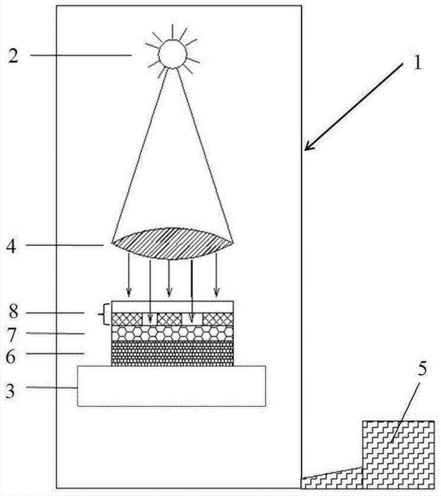
[0034] This embodiment provides a device for patterning nano-carbon material thin films, such as figure 1 As shown, it includes a closed working chamber 1, and the working chamber 1 is provided with an ultraviolet light source 2 and an operating table 3. The ultraviolet light source 2 is used to emit ultraviolet light with a wavelength band of 10-240nm and a wavelength band of 240-400nm. The operating table 3 is used for placing the nano-carbon material film 7 to be etched.

[0035] In this embodiment, an optical path collimation device 4 for optical path collimation is also arranged in the working chamber 1 , and the ultraviolet light is irradiated on the operation table 3 through the optical path collimation device 4 . The working chamber 1 is also connected with an ozone generator 5 , and the ozone generator 5 injects ozone into the sealed working chamber 1 .

[0036] The optical path collimation device 4 is similar to the exposure machine, and is selected from but not lim...

Embodiment 2

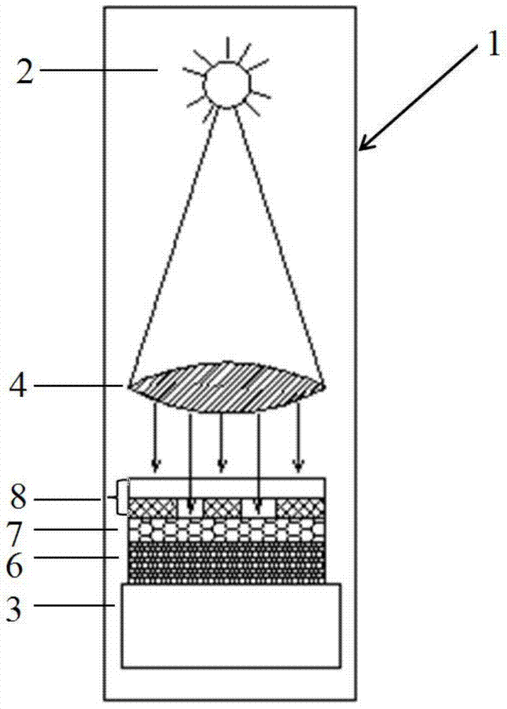
[0051] This embodiment provides a device for patterning nano-carbon material thin films, such as figure 2 As shown, the structure is the same as in Embodiment 1, except that the ozone generator 5 is not provided.

Embodiment 3

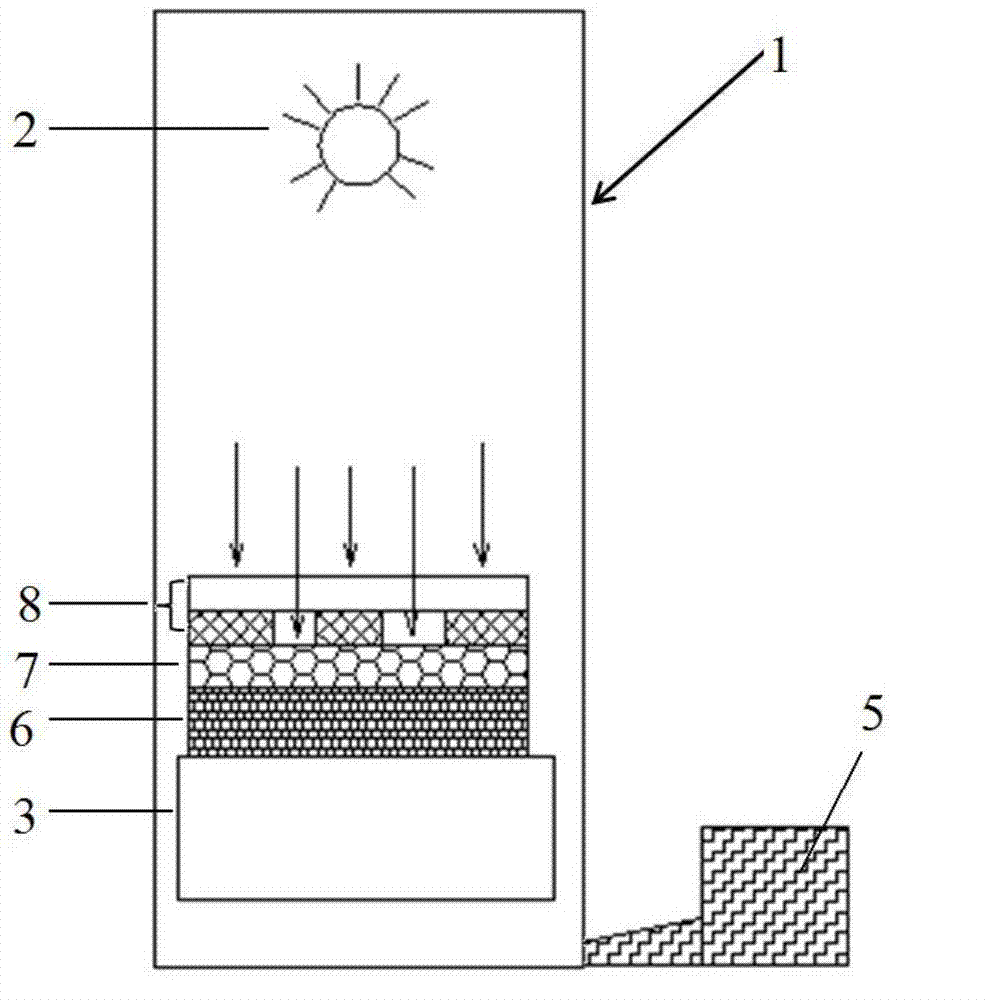
[0053] This embodiment provides a device for patterning nano-carbon material thin films, such as image 3 As shown, the structure is the same as that of Embodiment 1, except that the optical path collimation device 4 is not provided.


PUM

PropertyMeasurementUnit
Wavelengthaaaaaaaaaa
Thicknessaaaaaaaaaa

Abstract

The invention provides a method for pattering a nano carbon material film. The method is that an area to be etched, of the nano carbon material film is irradiated by ultraviolet rays to generate active carbon atoms and ozone; active ozone can be decomposed from the ozone; the active ozone with high oxidizing effect reacts with active carbon atoms to generate volatile carbon monoxide or carbon dioxide within a short time, and thus the area to be etched, of the nano carbon material can be etched. The invention provides a device for pattering the nano carbon material film. The device comprises a working cavity, an ultraviolet source arranged in the working cavity, and an operation bench. The device is simple in structure, safe and easy to be operated during pattering the nano carbon material film, and free of pollution and has a wide application prospect.

Description

technical field [0001] The invention relates to the field of thin-film devices, in particular to a method and equipment for patterning a nano-carbon material thin film. Background technique [0002] Nano-carbon materials such as graphene and carbon nanotubes have unique structures and properties. Films composed of nano-carbon materials have good electrical conductivity, good light transmission, rich raw materials and good curling properties. They have great potential in the field of thin film devices. Very broad application prospects. [0003] The application of nano-carbon thin films in the field of thin film devices inevitably requires patterning process steps. In the prior art, photolithography and etching processes are mainly used to pattern the nano-carbon film. The lithography process steps are cumbersome and involve multiple cleaning processes, and the nano-carbon film is not suitable for ultrasonic cleaning and other physical cleaning methods with high impact, whic...

Claims


Application Information

Patent Timeline
IPC IPC(8): H01L21/02B82Y40/00
CPCB82Y40/00H01L21/02H01L21/02527H01L21/02664
Inventor 祝晓钊
Owner KUNSHAN GO VISIONOX OPTO ELECTRONICS CO LTD
Why Eureka
Try Eureka