PECVD film coating method

A conventional, gas flow technology, applied in the direction of gaseous chemical plating, coating, electrical components, etc., can solve the problems of the decrease of the minority carrier life of the silicon wafer, the deterioration of the surface passivation effect, and the easy fracture, so as to reduce the electrical loss, Effect of increasing production cost and reducing package loss of components

Inactive Publication Date: 2015-07-08
HENGDIAN GRP DMEGC MAGNETICS CO LTD
View PDF5 Cites 3 Cited by
  • Summary
  • Abstract
  • Description
  • Claims
  • Application Information

AI Technical Summary

Problems solved by technology

The SiN:H film passivation used in conventional crystalline silicon solar energy is easily broken during the annealing process and the Si-H bond of the component under ultraviolet irradiation, resulting in the escape of H, which makes the surface passivation effect worse
At high temperature, a layer of SiO is thermally grown on the surface of the silicon wafer. 2 film, because the Si-O valence bond at the interface between silicon dioxide and silicon matches, the interface state can be reduced a lot, but because thermal growth of silicon dioxide is a high-temperature process, the passivation temperature is usually above 900 ° C, and high temperature is easy to make Defects are generated inside the silicon, resulting in a decrease in the minority carrier lifetime of the silicon wafer

Method used


Image

  • PECVD film coating method

Examples


Embodiment 1

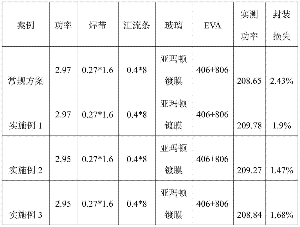
[0017] 125mm×125mm single crystal silicon wafer, using conventional process for texturing, diffusion and etching to remove phospho-silicate glass, anti-reflection coating using SiO 2 +SiNx coating process: deposit SiO first 2 Layer: deposition time 50s, SiH 4 Flow 300sccm, NH 3 Flow 2500sccm, N 2 O flow 2500sccm, pressure 1500mtor, power 3000W; re-deposit the first layer of SiNx: deposition time 170s, SiH 4 Flow 700sccm, NH 3 Flow rate 4300sccm, pressure 1700mtor, power 3000W; deposit the second layer of SiNx: deposition time 600s, SiH 4 Flow 450sccm, NH 3 The flow rate is 4500sccm, the pressure is 1700mtor, and the power is 4000W. After the coating is completed, the electrodes are printed and the electrical properties are tested, and cells of the same color and grade are selected to be packaged into components to test the electrical properties. The encapsulation loss of the cell assembly is shown in Table 1.

Embodiment 2

[0019] 125mm×125mm single crystal silicon wafer, using conventional process for texturing, diffusion and etching to remove phospho-silicate glass, anti-reflection coating using SiO 2 +SiNx coating process: deposit SiO first 2 Layer: deposition time 80s, SiH 4 Flow 300sccm, NH 3 Flow 2500sccm, N 2 O flow 2500sccm, pressure 1500mtor, power 3000W; re-deposit the first layer of SiNx: deposition time 170s, SiH 4 Flow 700sccm, NH 3 The flow rate is 4300sccm, the pressure is 1700sccm, and the power is 3000W; the second layer of SiNx is deposited: the deposition time is 540s, the flow rate of SiH4 is 450sccm, NH 3 The flow rate is 4500sccm, the pressure is 1700mtor, and the power is 4000W. After the coating is completed, the electrodes are printed and the electrical properties are tested, and cells of the same color and grade are selected to be packaged into components to test the electrical properties. The encapsulation loss of the cell assembly is shown in Table 1.

Embodiment 3

[0021] 125mm×125mm monocrystalline silicon wafer, using normal process for texturing, diffusion and etching to remove phospho-silicate glass, anti-reflection coating using SiO 2 +SiNx coating process: deposit SiO first 2 Layer: Deposition time 110s, SiH 4 Flow 200sccm, NH 3 Flow 3500sccm, N 2 O flow 2500sccm, pressure 1500mtor, power 3000W; re-deposit the first layer of SiNx: deposition time 170s, SiH 4 Flow 700sccm, NH 3 Flow rate 4300sccm, pressure 1700mtor, power 3000W; deposit the second layer of SiNx: deposition time 600s, SiH 4 Flow 450sccm, NH 3 The flow rate is 4500sccm, the pressure is 1700mtor, and the power is 4000W. After the coating is completed, the electrodes are printed and the electrical properties are tested, and cells of the same color and grade are selected to be packaged into components to test the electrical properties. The encapsulation loss of the cell assembly is shown in Table 1.

[0022] Table 1

[0023]

[0024] As shown in Table 1, by com...


PUM

PropertyMeasurementUnit
refractive indexaaaaaaaaaa

Abstract

The invention discloses a PECVD film coating method capable of reducing solar cell module packaging loss. The PECVD film coating method is characterized in that by a conventional crystalline silicon solar cell manufacturing technology, based on arrangement of a N2O gas passage on conventional PECVD equipment, an antireflection film containing SiO2 and SiNx is deposited on PECVD, and the film coating method comprises 1, SiO2 layer deposition: under the conditions of a certain pressure and power, feeding 4200-10800sccm of SiH4, NH3 and N2O into equipment and carrying out deposition for some time, and 2, SiNx layer deposition: carrying out two-step deposition to obtain a first SiNx layer and a second SiNx layer, under conditions of the same certain pressure and power, feeding different flows of SiH4 and NH3 into the equipment and carrying out deposition for some time. The PECVD film coating method has the advantages that based on arrangement of the N2O gas passage on the conventional PECVD equipment, the antireflection film containing SiO2 and SiNx is deposited on PECVD, through control of thickness and refractive indexes of the two films, light absorption is improved, and through use of SiO2 physical stability, electricity loss is reduced, module packaging loss is reduced, a production cost is not increased and feasibility is high.

Description

technical field [0001] The invention relates to the relevant technical field of high-efficiency solar cell components, in particular to a PECVD coating method capable of reducing packaging losses of solar cell components. Background technique [0002] With the development of crystalline silicon solar cell technology so far, the cost of power generation has become the main factor restricting the development of photovoltaic power generation. Reducing production costs and replacing low-efficiency batteries with high-efficiency batteries to obtain more energy has always been a hot topic in scientific research. In recent years, great achievements have been made in the research of high-efficiency single crystal battery technology, and the conversion efficiency of high-efficiency cells commercialized in the United States, Germany and Japan exceeds 20%. The current research results show that the reasons that affect the conversion efficiency of high-efficiency crystalline silicon so...

Claims


Application Information

Patent Timeline
Patent Type & Authority Applications(China)
IPC IPC(8): C23C16/52C23C16/34H01L31/18
CPCY02P70/50
Inventor 董方李虎明孙涌涛张向斌胡玉婷
Owner HENGDIAN GRP DMEGC MAGNETICS CO LTD
Why Eureka
Try Eureka